In the architecture of digital systems, information flow is governed by time. A timing diagram is not merely a drawing; it is a contract between design intent and physical implementation. When signals do not align within precise temporal windows, race conditions emerge, data corruption occurs, and system reliability collapses. This guide provides a rigorous framework for validating timing models, ensuring that every transition, edge, and constraint reflects the operational reality of the hardware.
Accuracy in timing representation is the difference between a functional prototype and a field failure. Whether defining a communication protocol or specifying register behavior, the clarity of the timing diagram dictates the success of the verification and implementation phases. This checklist outlines the critical elements required to maintain high fidelity in your timing models.
Why Timing Diagram Accuracy Matters 🎯
Timing diagrams serve as the primary reference for engineers during the implementation of finite state machines, bus protocols, and interface logic. They translate abstract logic into temporal constraints that physical silicon must obey. Inaccuracies in these models often stem from oversimplified representations of asynchronous events or undefined signal states.
Errors in timing documentation propagate through the entire development lifecycle. A mismatched clock edge definition can lead to setup violations. An ambiguous reset polarity can cause a system to boot into an undefined state. The cost of correcting a timing error during the design phase is significantly lower than the cost of a silicon re-spin or a firmware patch deployed to the field.
Key reasons for maintaining strict accuracy include:
- Verification Alignment: Simulation testbenches rely on these diagrams to generate stimulus. If the diagram is wrong, the testbench validates incorrect behavior.
- Implementation Consistency: Hardware description language code must match the timing specification. Discrepancies lead to synthesis warnings and timing closure failures.
- Interoperability: When interfacing with external components, timing margins ensure reliable communication between different systems.
- Debugging Efficiency: When a system fails, accurate timing diagrams provide a baseline for root cause analysis.
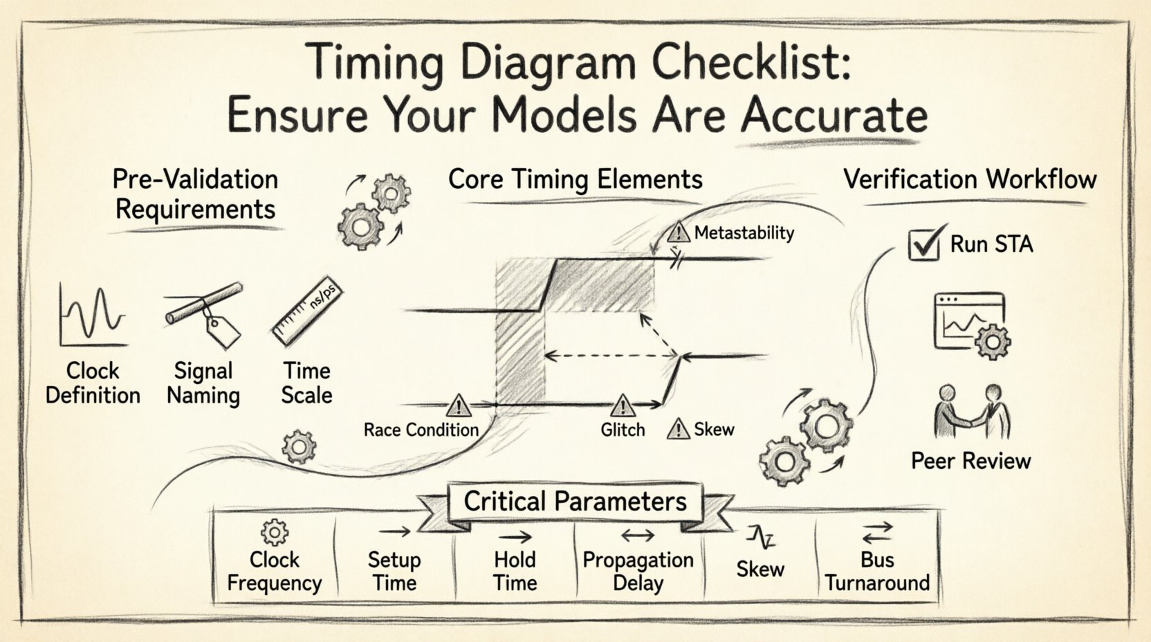
Pre-Validation Requirements ✅
Before reviewing the diagram itself, the context surrounding the signals must be established. A diagram without context is a collection of lines that hold little meaning. Ensure the following foundational elements are defined before proceeding to the signal-level checklist.
1. System Clock Definition
Every synchronous system relies on a clock source. The diagram must explicitly state the frequency, phase relationship, and duty cycle. Ambiguity here leads to clock domain crossing issues.
- Is the clock frequency specified in Hertz?
- Are there multiple clock domains? If so, are they labeled distinctly?
- Is the clock edge defined (rising or falling) for all sequential elements?
2. Signal Naming Conventions
Consistency in naming prevents misinterpretation during code implementation. Signals should follow a standard convention that indicates type, direction, and polarity.
- Use active-high or active-low indicators consistently.
- Ensure bus signals are grouped logically (e.g., DATA[7:0]).
- Avoid generic names like Sig1 or Ctrl without context.
3. Time Scale and Units
The horizontal axis represents time. Without clear units, the diagram becomes useless for timing analysis.
- Specify the time unit (ns, ps, µs, clock cycles).
- Ensure the scale is linear unless the diagram explicitly denotes a zoomed-in view of a specific event.
- Mark time markers at regular intervals to facilitate measurement.
Core Timing Elements Checklist 📋
This section details the specific signal characteristics that must be verified. Each element represents a potential point of failure if not explicitly defined.
1. Signal States and Levels
Digital signals exist in discrete states. The diagram must clearly depict what constitutes a logical one and a logical zero, as well as high-impedance states.
- Logic Levels: Are voltage levels or logic states (0/1) used? Ensure consistency throughout the document.
- High-Z State: For tri-state buses, the diagram must show the transition to the high-impedance state. This is critical for preventing bus contention.
- Undefined States: If a signal can enter a floating or unknown state, it must be marked. Do not assume a default value.
2. Transition Edges
The moment a signal changes state is the most critical moment in digital logic. Timing violations often occur at these edges.
- Rising Edge: Clearly mark the transition from low to high.
- Falling Edge: Clearly mark the transition from high to low.
- Slew Rate: While often abstracted, the steepness of the transition can affect timing margins. Indicate if slow transitions are expected due to load capacitance.
- Glitches: If a signal is prone to transient glitches, indicate them explicitly. Do not draw a clean line if the signal is noisy.
3. Setup and Hold Times
For flip-flops and latches, data must be stable before and after the active clock edge. These constraints are non-negotiable in synchronous design.
- Setup Time (tsu): The minimum time data must be stable before the clock edge.
- Hold Time (th): The minimum time data must remain stable after the clock edge.
- Violation Margins: Include safety margins in the diagram to account for process variations and temperature changes.
4. Latency and Delays
Signal propagation is not instantaneous. Delays accumulate across logic gates and interconnects.
- Specify propagation delays between input and output.
- Account for combinatorial logic delays in the path.
- Indicate if delays are worst-case, typical, or best-case.
Signal Integrity and Levels 🔌
Signal integrity encompasses the quality of the signal as it travels through the system. In timing diagrams, this is often represented by the clarity of the waveform.
1. Noise and Jitter
Real-world signals are subject to noise. A timing diagram that shows perfect edges is theoretically useful but practically misleading.
- Jitter: Variations in the timing of a signal edge. High jitter can reduce the effective timing margin.
- Noise Floor: If the signal operates near a noise threshold, the diagram should reflect the uncertainty band.
- Sampling Windows: Define the window within which the receiver samples the signal. This window must accommodate jitter.
2. Power Supply Dependencies
Signal timing can vary based on voltage levels. Power fluctuations can cause timing drift.
- Specify the operating voltage range for the components involved.
- Indicate if timing constraints change under different voltage conditions (e.g., low voltage operation).
- Consider power-down and power-up sequences in the timing model.
Table: Critical Timing Parameters Reference
| Parameter | Definition | Impact of Error | Verification Method |
|---|---|---|---|
| Clock Frequency | Rate of clock cycles per second | System speed mismatch, data loss | Frequency counter, Oscilloscope |
| Setup Time | Time data must be stable before clock edge | Metastability, incorrect data capture | Static Timing Analysis |
| Hold Time | Time data must be stable after clock edge | Metastability, data corruption | Static Timing Analysis |
| Propagation Delay | Time taken for signal to travel from input to output | Timing violations, race conditions | Simulation Waveforms |
| Skew | Difference in arrival time of clock to different registers | Reduced timing margin, clock domain issues | Clock Tree Analysis |
| Bus Turnaround Time | Time to switch from driver to receiver state | Bus contention, data collision | Signal Integrity Simulation |
Clock Domain and Synchronization ⏲️
Modern systems often operate across multiple clock domains. Crossing these boundaries introduces significant complexity that must be captured in the timing diagram.
1. Multi-Clock Scenarios
When signals cross from one clock domain to another, the relationship between the clocks must be defined.
- Frequency Ratio: Is one clock a multiple of the other?
- Phase Relationship: Are the clocks aligned, or is there a fixed phase offset?
- Asynchronous Clocks: If clocks are unrelated, the diagram must indicate the need for synchronization logic (e.g., synchronizers, FIFOs).
2. Metastability Handling
When asynchronous signals enter a synchronous system, they risk causing metastability. The timing diagram should account for the recovery time required.
- Specify the metastability recovery time.
- Indicate the use of multi-stage synchronizers.
- Define the probability of failure acceptable for the application.
3. Clock Gating
To save power, clocks are often gated off when logic is idle. This introduces timing complexities.
- Show the enable signal for the clock gate.
- Define the minimum pulse width required to trigger the gated clock.
- Ensure the gating logic does not introduce glitches.
State Transitions and Reset Logic 🔄
Logic behavior is defined by state transitions. The timing diagram must accurately reflect how the system moves between states and how it initializes.
1. Reset Sequence
Every digital system needs a defined start state. The reset signal is critical for this.
- Active Level: Is the reset active high or active low?
- Pulse Width: How long must the reset signal remain active to ensure all registers clear?
- Release Order: If multiple reset signals exist, is there a specific release order? (e.g., core reset before I/O reset).
- Asynchronous vs. Synchronous: Does the reset clear immediately or on the next clock edge?
2. State Machine Transitions
Finite State Machines (FSM) define the operational logic. The timing diagram should map out the transition conditions.
- Identify the input conditions that trigger a state change.
- Show the duration of the output associated with each state.
- Highlight any illegal states and how the system handles them.
3. Handshake Protocols
Many interfaces use handshakes to manage data flow. The timing of these signals is vital.
- Request (REQ): When is the data ready to be sent?
- Acknowledge (ACK): When does the receiver confirm receipt?
- Timeout: What happens if the handshake does not complete within a certain time?
Verification and Cross-Checking 🔍
Once the diagram is drafted, it must undergo a rigorous review process. This involves comparing the diagram against simulation results and physical constraints.
1. Simulation Waveform Comparison
Run a simulation using the timing constraints defined in the diagram. Compare the actual output waveforms against the planned diagram.
- Do the signal edges align with the clock edges as expected?
- Are the setup and hold times met in the simulation?
- Do the data values match the expected sequence?
2. Static Timing Analysis (STA)
STA tools analyze the timing paths without running simulations. They provide a mathematical proof of timing correctness.
- Check for timing violations reported by the STA engine.
- Review the slack values for critical paths.
- Ensure the timing constraints in the diagram match the constraints files used by the analysis tool.
3. Peer Review
Human review is essential to catch logical errors that tools might miss.
- Have a second engineer review the diagram for clarity and consistency.
- Check for naming conventions and unit consistency.
- Verify that the diagram matches the architectural specification.
Common Timing Violations 🚫
Even with a checklist, errors occur. Familiarity with common pitfalls helps in prevention and troubleshooting.
1. Race Conditions
Occurs when the output of one signal depends on the order in which other signals arrive.
- Avoid logic where two signals drive the same node with different timing.
- Ensure feedback loops are broken or properly synchronized.
- Check for logic paths with vastly different delays feeding into the same register.
2. Metastability
When a signal changes too close to the clock edge, the flip-flop may not resolve to a 0 or 1.
- Minimize the probability of asynchronous inputs hitting the sampling edge.
- Use synchronizers for any external inputs.
- Design for worst-case jitter and skew.
3. Glitches
Unintended pulses caused by logic propagation delays.
- Ensure that combinational logic does not feed directly into sensitive control lines.
- Use clock gating logic that prevents glitches from reaching the clock tree.
- Verify that enable signals are stable before the clock edge.
4. Clock Skew
The clock arrives at different registers at different times.
- Minimize skew in the clock distribution network.
- Account for skew in the setup and hold time calculations.
- Use buffered clock trees to maintain uniformity.
Documentation and Maintenance 📝
A timing diagram is a living document. As the design evolves, the diagram must be updated to reflect changes.
1. Version Control
Keep track of changes to the timing diagram over time.
- Include a revision history table in the documentation.
- Version control the diagram files alongside the code.
- Log the reason for each change (e.g., “Updated to reflect new clock frequency”).
2. Contextual Notes
Add notes to the diagram to explain complex behaviors.
- Use text boxes to explain specific timing windows.
- Reference related sections of the specification.
- Include warnings about critical constraints.
3. Handoff to Implementation
Ensure the team building the system has the correct version of the diagram.
- Provide the diagram in a format accessible to all stakeholders.
- Conduct a walkthrough session with the implementation team.
- Collect feedback from the implementation team to improve future diagrams.
Final Thoughts on Timing Rigor 🛡️
Creating an accurate timing diagram is a discipline that requires attention to detail and a deep understanding of the underlying technology. It is not enough to draw lines; one must understand the physics and logic that govern those lines. By adhering to this checklist, you ensure that your models are robust, reliable, and ready for implementation.
The effort invested in validating timing diagrams pays dividends in reduced debugging time and higher system quality. In an industry where margins are tight and costs are high, precision is the most valuable asset you possess. Treat every edge and every delay with the seriousness it demands.
Remember, the diagram is the source of truth. If the diagram is wrong, the design is wrong. Keep the diagram accurate, keep the design functional, and keep the system running smoothly.