Understanding the flow of signals within a digital system is critical for engineers working on hardware, firmware, or embedded software. A timing diagram serves as the primary visual tool for mapping out how different signals interact over a specific period. This visual representation allows teams to verify that data is captured correctly, clocks are stable, and logic transitions occur without conflict. Without a precise understanding of these diagrams, system reliability can suffer significantly. This guide explores the essential elements that make up a timing diagram, ensuring accurate design and analysis.
What is a Timing Diagram? 📊
A timing diagram is a graphical illustration that shows the behavior of two or more signals over time. It maps the sequence of events, indicating when signals change state, how long they stay in that state, and how they relate to a clock source. In hardware design, these diagrams are indispensable for verifying that components communicate correctly. In software, they help visualize concurrency, race conditions, and synchronization points.
These diagrams typically plot time on the horizontal axis (x-axis) and signal level or state on the vertical axis (y-axis). The vertical lines represent specific points in time, while horizontal lines indicate the steady state of a signal. The transitions between these states are crucial, as they indicate the actual data transfer or control actions occurring within the system.
Core Components of a Timing Diagram 🔧
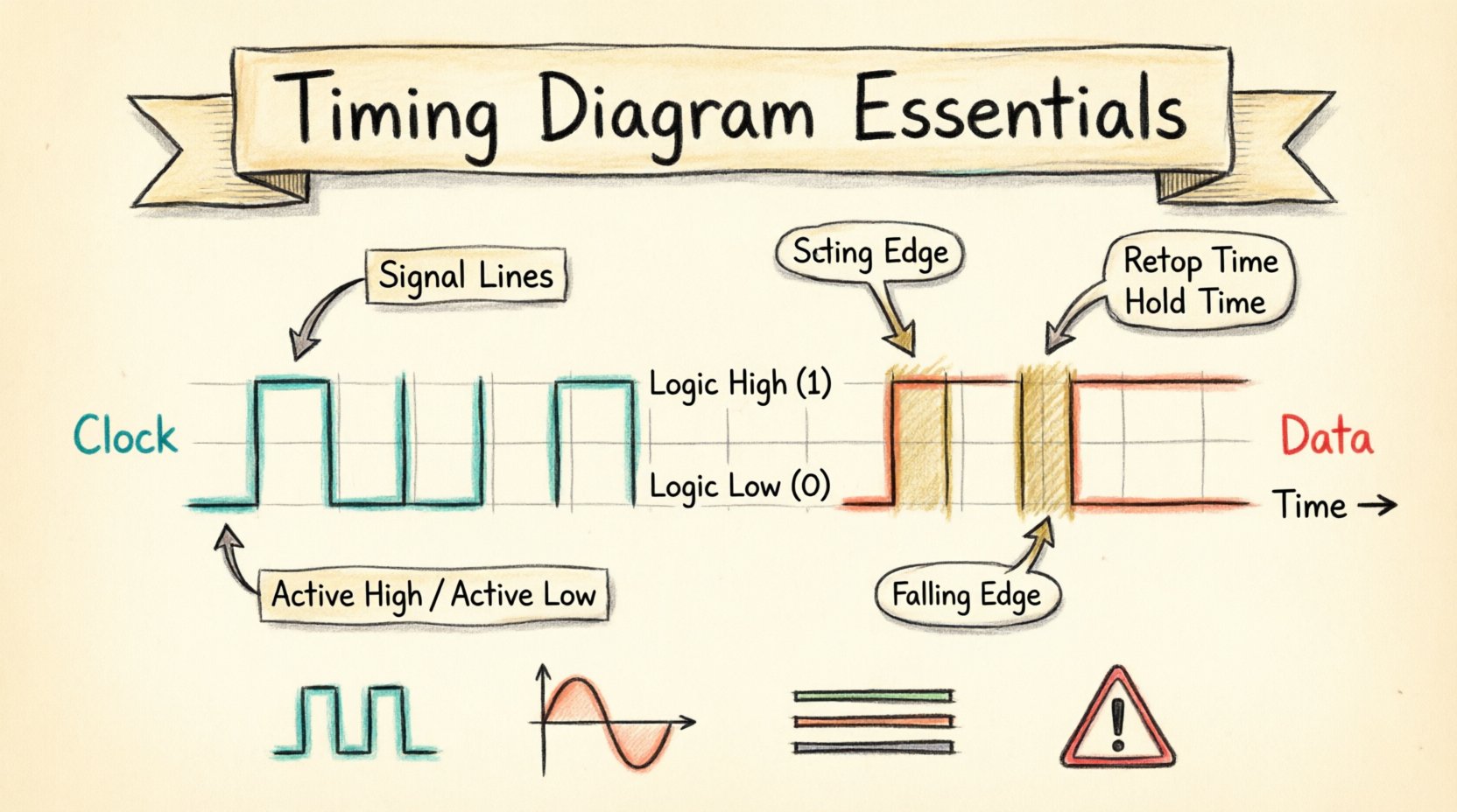
To read or create an effective timing diagram, one must understand the fundamental building blocks. Every diagram, regardless of complexity, relies on a consistent set of elements to convey information accurately.
- Time Axis: The horizontal baseline representing the progression of time. It usually flows from left to right, indicating “past” to “future”.
- Signal Lines: Horizontal tracks assigned to specific wires, buses, or variables. Each line represents the logic level of a specific signal.
- Logic Levels: The vertical positions on the signal line. Typically, high (1, Vcc, True) and low (0, Gnd, False) states are shown.
- Transitions: The vertical lines connecting logic levels. A rising edge moves from low to high, while a falling edge moves from high to low.
- Annotations: Text labels or markers that clarify specific events, delays, or states.
The Time Axis: Precision Matters ⏳
The time axis is the foundation of the diagram. It does not always represent real-world seconds; often, it represents clock cycles or nanoseconds depending on the design speed. Consistency in scaling is vital. If one section of the diagram shows 10 nanoseconds per grid square, another section must maintain that scale unless it is explicitly zoomed in for detail.
When analyzing system performance, the time axis helps identify bottlenecks. For example, if a data signal requires 50 nanoseconds to stabilize but the clock edge occurs after 40 nanoseconds, a violation exists. The axis allows engineers to measure these intervals directly.
Signal Lines and Logic Levels 🔄
Each signal line corresponds to a physical wire or a logical variable. In complex systems, a bus might be represented by a thick line with multiple signals grouped together, or individual lines for each bit. The logic levels define the state of the signal:
- Active High: The signal is considered “on” or “true” when the voltage is high.
- Active Low: The signal is considered “on” or “true” when the voltage is low. This is often indicated with a bubble on the symbol or a specific naming convention.
Understanding the active state is crucial for interpreting control signals like “Chip Select” or “Write Enable.” Misinterpreting an active-low signal as active-high can lead to design failures that are difficult to debug.
Transitions and Edges ⚡
Transitions occur when a signal changes from one logic level to another. These changes are rarely instantaneous in the physical world, but in a timing diagram, they are often drawn as vertical lines to represent the ideal moment of change.
- Rising Edge: The transition from low to high. This is often the trigger point for synchronous logic.
- Falling Edge: The transition from high to low. Some systems use this edge for data capture.
- Edge-Triggered: Logic that responds only at the moment of the transition.
- Level-Triggered: Logic that responds as long as the signal remains in a specific state.
Real-world signals have rise and fall times. A perfect vertical line is an abstraction. In high-speed designs, the slope of the transition matters because it affects electromagnetic interference and signal integrity.
Timing Parameters and Constraints 📐
Beyond the visual lines, the critical value of a timing diagram lies in the quantitative parameters defined alongside the signals. These parameters dictate the physical limits within which the hardware must operate.
Setup and Hold Time ⚙️
These are the two most common constraints in sequential logic design, particularly when data is being captured by a flip-flop on a clock edge.
- Setup Time: The minimum amount of time the data signal must be stable before the active clock edge. If data changes too close to the clock edge, the flip-flop may not capture the correct value.
- Hold Time: The minimum amount of time the data signal must remain stable after the active clock edge. If the data changes too soon after the edge, the capture may be corrupted.
| Parameter | Definition | Consequence of Violation |
|---|---|---|
| Setup Time | Time data must be stable before clock edge | Metastability or incorrect data capture |
| Hold Time | Time data must be stable after clock edge | Metastability or incorrect data capture |
| Propagation Delay | Time taken for signal to travel through a gate | Timing slack reduction, slower max frequency |
| Clock Skew | Difference in arrival time of clock signal | Effective timing window reduction |
Propagation Delay ⏱️
Propagation delay is the time it takes for a change in input to affect the output. In a timing diagram, this is visible as the gap between a clock edge and the resulting data change. This delay is caused by physical limitations, such as capacitance in the wires and the switching speed of transistors.
When designing a system, the sum of propagation delays along a path must be less than the clock period minus the setup time. If the delay is too long, the system cannot run at the desired clock speed.
Clock Skew and Jitter 📉
Clock skew refers to the difference in arrival times of the clock signal at different parts of the circuit. In an ideal diagram, the clock line is vertical and simultaneous for all components. In reality, routing differences cause skew. Positive skew means the clock arrives later at the destination, which can help with setup time but hurts hold time.
Jitter is the variation in the timing of the signal edges. It is noise that causes the edge to occur earlier or later than expected. High jitter reduces the effective timing margin, requiring the system to run slower to maintain stability.
Types of Signals and Buses 📡
Different systems use different signaling methods. The timing diagram must reflect these differences to be accurate.
Digital Signals
Most timing diagrams focus on digital logic. These signals are binary, switching between 0 and 1. The clarity of the diagram depends on clearly marking the logic thresholds. Some signals may have intermediate states or “don’t care” conditions, usually marked with an X.
Analog Signals
While less common in pure digital timing diagrams, analog signals like voltage rails or sensor outputs are sometimes included. These are represented with sloped or curved lines rather than sharp steps, indicating continuous variation rather than discrete state changes.
Buses and Parallel Data
When multiple bits travel simultaneously, they are often grouped. A bus timing diagram shows the state of all bits at once. It is essential to label the bus width (e.g., 8-bit, 32-bit) and show the valid data window where all bits are stable simultaneously.
Reading a Timing Diagram: A Step-by-Step Guide 🔍
Interpreting these diagrams requires a systematic approach to avoid missing critical details.
- Identify the Clock: Locate the primary timing reference. All other events should be measured relative to this line.
- Determine Edge Sensitivity: Check if the system triggers on the rising or falling edge of the clock.
- Trace Data Validity: Look for the period where data lines are stable. This is the “valid window”.
- Check Control Signals: Identify enable, reset, or chip select lines that gate the data transfer.
- Measure Intervals: Use the time axis to measure delays, setup times, and pulse widths.
Common Timing Violations and Errors ⚠️
Even with careful planning, timing violations occur. Recognizing the signs in a diagram is the first step to fixing them.
- Setup Violation: Data arrives too late for the next clock edge. The solution often involves slowing the clock or optimizing the logic path to reduce delay.
- Hold Violation: Data changes too soon after the clock edge. This is often harder to fix because it may require adding delay to the data path or the clock path.
- Metastability: A state where a flip-flop output is neither 0 nor 1 for an undefined period. This usually happens when setup or hold times are violated.
- Glitches: Short, unintended pulses caused by race conditions in combinational logic. These can trigger false state changes if not filtered.
Asynchronous vs. Synchronous Design 🔄
Timing diagrams look different depending on the design methodology.
Synchronous Design
Events are coordinated by a global clock. The timing diagram shows clear, periodic clock lines. Data changes only at clock edges. This approach simplifies analysis because the timing window is fixed.
Asynchronous Design
Events are coordinated by handshake signals (like Request and Acknowledge). The timing diagram shows irregular intervals between events. While more flexible, these diagrams are harder to analyze because there is no fixed time reference.
Application in Protocols 📡
Communication protocols rely heavily on precise timing. Understanding the diagram is key to implementing these standards.
Serial Communication
Serial interfaces send data one bit at a time. The timing diagram shows the bit period. The relationship between the clock and the data line (e.g., data valid on the rising edge) defines the protocol rules.
Parallel Communication
Parallel interfaces send multiple bits at once. The timing diagram must show the setup time for the entire bus. All bits must be stable before the latch edge occurs.
Best Practices for Documentation 📝
Creating clear documentation ensures that other engineers can understand the system without ambiguity.
- Use Consistent Labels: Name signals exactly as they appear in the code or schematic.
- Include Units: Always specify the time units (ns, µs, cycles) on the axis.
- Highlight Critical Paths: Use bold lines or colors to indicate the most timing-sensitive signals.
- Annotate Violations: If a violation is known, mark it clearly rather than hiding it.
- Keep It Current: Update diagrams whenever the design changes. Outdated diagrams are a major source of bugs.
Advanced Considerations: Multi-Clock Domains 🌐
Modern systems often operate with multiple clock domains running at different speeds. A timing diagram for these systems must clearly show the relationship between the clocks.
- Cross-Clock Transitions: Data moving from a fast domain to a slow domain requires careful synchronization to avoid data loss.
- Phase Relationships: If two clocks share a source but have different phases, the diagram must show the phase shift.
- Handshake Logic: Asynchronous bridges between domains rely on handshake signals. The timing diagram must show the full request-acknowledge cycle.
The Role of Simulation in Timing Analysis 💻
Before hardware is built, simulations verify the timing diagrams. Engineers use waveform viewers to compare expected behavior against simulated results.
- Static Timing Analysis: Calculates worst-case delays without simulating actual waveforms.
- Dynamic Timing Simulation: Runs a virtual version of the circuit to generate actual waveforms.
- Post-Layout Simulation: Accounts for physical wire lengths and capacitance after the chip is designed.
These tools allow engineers to validate the timing diagram against physical reality. If the simulation shows a setup violation, the design must be revised before fabrication.
Conclusion on Timing Accuracy ✅
Mastering the creation and interpretation of timing diagrams is a fundamental skill for technical professionals. These diagrams bridge the gap between abstract logic and physical reality. They ensure that signals arrive when needed, in the correct state, and with enough stability for the system to function. By adhering to the elements and constraints outlined in this guide, teams can reduce errors and improve system reliability. Attention to detail in these visual representations pays dividends in the stability and performance of the final product.
Whether working on high-speed memory interfaces, low-power microcontrollers, or complex data buses, the principles remain the same. Time is the constant, and the signals are the variables. Understanding their relationship is the key to successful engineering.