Timing diagrams are essential tools for visualizing the behavior of digital signals over a specific period. In the field of digital electronics and computer engineering, understanding how signals interact is critical for system stability and performance. This guide provides a detailed examination of timing diagram notation, ensuring you can read, create, and interpret waveforms with precision. We will explore signal levels, time axes, transitions, and critical timing parameters without relying on specific software tools.
🔍 Understanding the Core Components of Timing Diagrams
At its foundation, a timing diagram represents the logical state of signals relative to time. It acts as a blueprint for how data moves through a system. To interpret these diagrams correctly, one must understand the fundamental axes and signal representations.
- Horizontal Axis: Represents time. This axis flows from left to right, indicating the sequence of events.
- Vertical Axis: Represents the logic state or voltage level of a specific signal line.
- Signal Lines: Each horizontal line corresponds to a specific wire, net, or logical variable within the circuit.
- Logic Levels: Signals generally toggle between two states, typically referred to as High and Low.
When analyzing a timing diagram, the viewer looks for the relationship between changes in one signal and changes in another. This relationship determines whether data is captured correctly or if errors occur. Proper notation ensures that these relationships are unambiguous to engineers reviewing the design.
⚡ Signal Logic Levels and States
Digital systems operate on binary principles, but the physical representation varies. Notation must clearly define what constitutes a logical one and a logical zero. Misinterpreting these levels can lead to catastrophic design failures.
Active High vs. Active Low
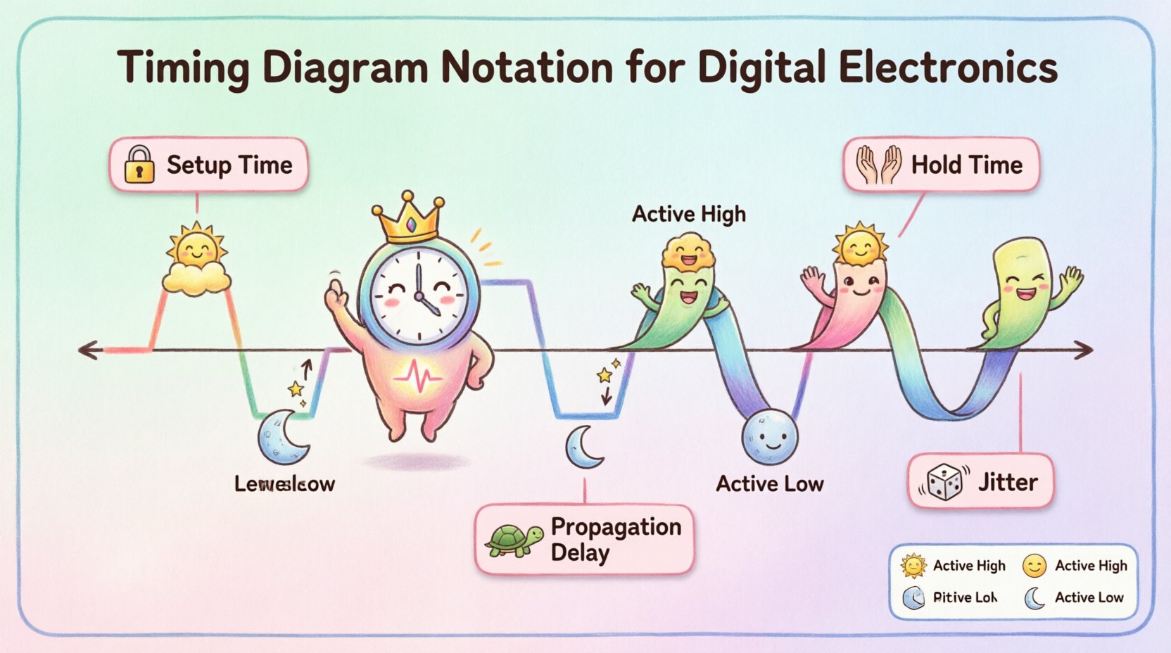
Signals can be active when they are high or active when they are low. This concept is vital for control signals like resets or enables.
- Active High: The signal performs its function when the voltage is high (logic 1). This is the standard for most data lines.
- Active Low: The signal performs its function when the voltage is low (logic 0). Control signals often use this notation to reduce noise or match specific hardware requirements.
- Notation Indicators: Active low signals are often marked with a bar over the name or a bubble at the end of the line in schematic diagrams.
Logic Voltage Levels
While logic 0 and 1 are abstract, the timing diagram represents physical voltages. The notation should ideally specify the voltage thresholds.
- Logic High: Typically represented by a voltage above a specific threshold (e.g., 3.3V or 5V).
- Logic Low: Typically represented by a voltage below a specific threshold (e.g., 0V).
- Undefined Zone: The area between the high and low thresholds where the signal state is indeterminate. Diagrams should avoid resting in this zone.
⏱️ Time Axis and Synchronization
The representation of time is the second most critical aspect of timing diagrams. Unlike voltage, time is continuous, but digital signals change at discrete moments. The notation must handle both synchronous and asynchronous events.
Clock Signals
Most digital systems rely on a clock to synchronize operations. The clock signal is the heartbeat of the system.
- Period: The time it takes for one complete cycle of the clock.
- Frequency: The number of cycles per second, usually measured in Hertz.
- Duty Cycle: The percentage of the period where the signal is high.
- Notation: Clock signals are often drawn with a square wave pattern.
Relative vs. Absolute Time
Timing diagrams can use relative time or absolute time.
- Relative Time: Measurements are taken from a reference point, such as a specific clock edge. This is common for setup and hold time analysis.
- Absolute Time: Specific timestamps are assigned to events, useful for debugging communication protocols over long durations.
Time Scales
Choosing the correct time scale is crucial for clarity.
- Nanoseconds: Used for high-speed logic where signals change rapidly.
- Microseconds: Used for slower peripheral interactions.
- Milliseconds: Used for system-level power management or low-frequency events.
🔄 Edge Transitions and Notation
The moment a signal changes state is just as important as the state itself. Notation must clearly depict how and when these transitions occur.
Rising and Falling Edges
Edges represent the transition between logic levels.
- Rising Edge: The transition from Low to High. Often marked with a vertical line or an arrow pointing up.
- Falling Edge: The transition from High to Low. Often marked with a vertical line or an arrow pointing down.
- Slope: In ideal diagrams, edges are vertical. In real-world diagrams, edges have a slope representing rise time or fall time.
Transition Delays
Signals do not switch instantly. The notation must account for propagation delays.
- Propagation Delay: The time it takes for a change at the input to result in a change at the output.
- Notation: Often indicated by a gap between the input transition and the output transition.
Glitches and Hazards
Unintended transitions can occur due to circuit delays. These are often shown as brief spikes.
- Glitch: A short pulse that should not be there. Notation may use dashed lines or distinct colors.
- Hazard: A potential for incorrect output due to timing differences.
📏 Critical Timing Parameters
Certain parameters define the reliability of a digital interface. These are the metrics engineers measure to ensure data integrity.
| Parameter | Description | Unit |
|---|---|---|
| Setup Time | Time data must be stable before the clock edge. | Time (ns) |
| Hold Time | Time data must remain stable after the clock edge. | Time (ns) |
| Propagation Delay | Time from input change to output change. | Time (ns) |
| Clock-to-Q | Time from clock edge to output change. | Time (ns) |
| Jitter | Variation in the timing of a signal edge. | Time (ps/ns) |
Setup and Hold Times
These are the most critical constraints for synchronous systems.
- Setup Time Violation: If data changes too close to the clock edge, the system may not capture the correct value.
- Hold Time Violation: If data changes too soon after the clock edge, the system may lose the value.
- Notation: These are typically shown as windows of time around the clock edge where the data line must not change.
Propagation Delay
This delay affects the maximum frequency of the system.
- High-to-Low: Time taken for a signal to go from High to Low.
- Low-to-High: Time taken for a signal to go from Low to High.
- Notation: Often shown as a horizontal gap between the input and output waveforms.
🛠️ Control Signals and Active States
Control signals manage the flow of data. Their notation must clearly indicate when they are active.
| Signal Type | Active State | Notation Example |
|---|---|---|
| Reset | Active Low | Reset# or Reset_bar |
| Enable | Active High | Enable |
| Interrupt | Active High or Low | IRQ or IRQ_bar |
| Chip Select | Active Low | CS# |
Reset Signals
Reset signals initialize the system. They can be asynchronous or synchronous.
- Asynchronous Reset: Takes effect immediately, regardless of the clock. Notation shows the reset line going active at any time.
- Synchronous Reset: Takes effect only on a clock edge. Notation shows the reset line active before the clock edge.
Enable Signals
Enable signals allow or block operations.
- High Enable: Operation occurs when the signal is High.
- Low Enable: Operation occurs when the signal is Low.
📖 Reading and Analyzing Waveforms
Reading a timing diagram requires a systematic approach. Engineers should follow specific steps to avoid misinterpretation.
Step-by-Step Analysis
- Identify the Clock: Locate the primary timing reference. All synchronous events relate to this.
- Trace Data Flow: Follow the data lines from source to destination.
- Check Timing Windows: Verify setup and hold times against the clock edge.
- Look for Anomalies: Identify glitches, spikes, or unexpected transitions.
- Verify Logic Levels: Ensure active states match the component specifications.
Common Misinterpretations
- Assuming Instantaneous Change: Real signals have rise and fall times. Assuming vertical edges can hide timing violations.
- Ignoring Asynchronous Signals: Control signals that are not clocked can appear at any time and must be checked independently.
- Misreading Active States: Confusing Active High with Active Low is a common source of design errors.
🚀 Advanced Timing Considerations
As systems become faster, timing analysis becomes more complex. Advanced notation addresses these challenges.
Metastability
When a signal changes during the setup or hold window, the output may enter a metastable state.
- Definition: The signal settles at an intermediate voltage level.
- Notation: Often shown as a question mark or a shaded region between High and Low.
- Resolution: The signal eventually resolves to High or Low, but the time is unpredictable.
Synchronization Skew
Different paths may take different amounts of time to reach a destination.
- Clock Skew: The clock signal arrives at different components at different times.
- Data Skew: Data signals arrive at different destinations at different times.
- Notation: Shown as a horizontal offset between the expected and actual arrival times.
Jitter
Jitter is the deviation of the signal edge from its ideal position.
- Cycle-to-Cycle Jitter: Variation between one clock cycle and the next.
- Period Jitter: Variation in the total duration of the clock cycle.
- Notation: Often shown as a shaded area around the ideal edge position.
📝 Best Practices for Documentation
Creating clear timing diagrams ensures that others can understand your design. Adhering to best practices reduces ambiguity.
- Consistent Naming: Use clear, unique names for all signals. Avoid generic names like Signal1 or Signal2.
- Standard Symbols: Use standard notation for edges, levels, and delays to ensure industry compatibility.
- Clear Time Scales: Label the time axis explicitly with units (ns, µs, ms).
- Group Related Signals: Group signals that belong to the same protocol or subsystem together.
- Highlight Critical Times: Use bold lines or colors to highlight setup and hold windows.
- Provide Legends: Include a key for any custom symbols or abbreviations used in the diagram.
🔚 Summary of Key Takeaways
Timing diagram notation is a fundamental skill for anyone working in digital design. By understanding the core components, signal levels, and timing parameters, engineers can ensure robust system performance. Proper notation eliminates ambiguity and prevents costly design errors. Remember to focus on setup and hold times, clearly define active states, and account for real-world signal characteristics like propagation delay and jitter. Following these guidelines will result in clear, effective documentation.
When creating or reviewing these diagrams, always verify the logic levels against the hardware specifications. Ensure that the time axis reflects the actual operating frequency of the system. Finally, maintain consistency in your notation style across all documentation to facilitate collaboration. With practice, interpreting and creating these diagrams will become a natural part of the design workflow.
Final Notes on Implementation
While this guide covers the theoretical and notational aspects, practical implementation requires attention to the physical layer. Signal integrity, noise margins, and power delivery all influence the timing behavior. Always cross-reference timing diagrams with datasheets and simulation results to validate the design. Continuous learning and adherence to industry standards will keep your designs reliable and efficient.