In the intricate world of embedded engineering, precision is not merely a preference; it is a requirement. Timing diagrams serve as the visual blueprint for understanding how signals interact over time. These graphical representations map voltage levels, clock cycles, and data transitions against a temporal axis. For engineers designing microcontrollers, sensors, or communication interfaces, mastering the reading and creation of these diagrams is essential for ensuring system reliability.
Without a clear view of temporal relationships, hardware components may fail to communicate, leading to data corruption or system crashes. This guide explores the practical applications of timing diagrams across various domains within embedded development, offering a deep dive into their utility without relying on specific software tools.
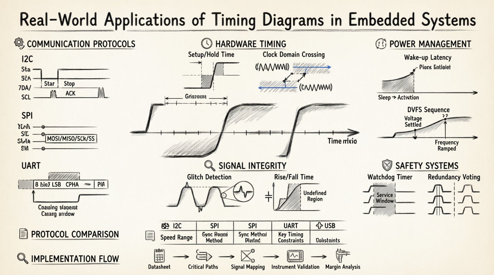
🔌 Communication Protocol Analysis
Serial communication is the backbone of modern embedded systems. Data rarely stays within a single chip; it moves between processors, memory, and peripherals. Timing diagrams are critical for defining and verifying these interactions.
Inter-Integrated Circuit (I2C)
The I2C protocol utilizes a two-wire interface: Serial Data (SDA) and Serial Clock (SCL). A timing diagram for I2C reveals the specific sequence required for data transmission.
- Start Condition: The SDA line transitions from high to low while the SCL line remains high. This signals the bus to begin a transaction.
- Address Frame: The first byte sent contains the 7-bit address of the target device plus a read/write bit.
- Acknowledgement: The receiver pulls the SDA line low during the ninth clock pulse to confirm receipt.
- Stop Condition: The SDA line transitions from low to high while SCL is high, releasing the bus.
Engineers use these diagrams to detect issues like clock stretching. If a slave device cannot process data quickly enough, it holds the SCL line low. The timing diagram shows this extension, allowing the designer to adjust processing loops or buffer sizes.
Serial Peripheral Interface (SPI)
SPI is a synchronous protocol often used for higher-speed communication. It involves four lines: Master Out Slave In (MOSI), Master In Slave Out (MISO), Serial Clock (SCK), and Slave Select (SS).
- Clock Polarity (CPOL): Determines the idle state of the clock line. Is it high or low before data starts?
- Clock Phase (CPHA): Defines when data is sampled. Is it on the first or second clock edge?
- Chip Select Timing: The SS line must remain low for the entire duration of the transaction. If it glitches high, the transaction aborts.
Understanding these phases is vital. A mismatch in CPOL or CPHA between master and slave results in garbage data. A timing diagram visualizes these edges, making it easy to spot mismatches during hardware bring-up.
Universal Asynchronous Receiver/Transmitter (UART)
Unlike SPI and I2C, UART does not use a clock line. Synchronization relies on agreed-upon baud rates. Timing diagrams here focus on the bit duration and framing.
- Start Bit: A low pulse indicates the beginning of a byte.
- Data Bits: Typically 8 bits, transmitted Least Significant Bit (LSB) first.
- Stop Bit: A high pulse signals the end of the byte.
Timing diagrams help engineers calculate the tolerance window. If the clocks of the two devices drift too far apart, the sampling point shifts, causing errors. The diagram illustrates the sampling window, usually centered in the middle of the bit time.
⏱️ Hardware Synchronization and Setup Times
Beyond communication, timing diagrams are indispensable for understanding how logic gates and flip-flops interact. Digital logic relies on precise timing constraints to function correctly.
Setup and Hold Times
When data enters a register or flip-flop, it must meet specific timing requirements relative to the clock edge.
- Setup Time: The minimum duration data must be stable before the clock edge arrives.
- Hold Time: The minimum duration data must remain stable after the clock edge arrives.
If a signal violates the setup time, the register might capture the wrong value. If it violates the hold time, metastability can occur. A timing diagram visualizes the data signal relative to the clock edge, highlighting the forbidden zones where data changes are not allowed.
Clock Domain Crossing (CDC)
Complex systems often run different parts of the logic at different clock frequencies. Moving data from a fast clock domain to a slow one, or vice versa, introduces risks.
- Synchronization: Using a chain of flip-flops to ensure the signal is stable before use.
- Handshaking: Using request and acknowledge signals to coordinate data transfer without a shared clock.
A timing diagram for CDC shows the handshake sequence. It ensures the data is valid before the receiving domain acknowledges it. This prevents data loss in asynchronous transfers.
🔍 Debugging and Signal Integrity
When an embedded system behaves unexpectedly, timing diagrams are often the first place engineers look. They provide a historical record of signal behavior that static testing cannot capture.
Identifying Glitches
A glitch is a brief, unintended pulse on a signal line. It might last only a few nanoseconds but can trigger a state change in a flip-flop.
- Race Conditions: Occur when the order of events matters, and timing is too tight.
- Propagation Delay: Signals take time to travel through logic gates. Timing diagrams show these delays clearly.
By overlaying the expected timing diagram with the captured actual signals, engineers can pinpoint exactly where the deviation occurs. This allows for targeted fixes in the firmware or hardware design.
Noise Margins and Rise/Fall Times
Real-world signals are not perfect square waves. They have rise and fall times due to capacitance and inductance in the traces.
- Rise Time: The time taken for a signal to transition from low to high.
- Fall Time: The time taken for a signal to transition from high to low.
If these transitions are too slow, the signal might spend too much time in the undefined voltage region between logic 0 and logic 1. This can cause multiple clock edges to be triggered or logic errors. A timing diagram helps measure these slopes to ensure they meet the specifications of the receiving chip.
💤 Power Management and Low Power States
Energy efficiency is a major concern in battery-operated embedded devices. Timing diagrams play a role in optimizing power consumption.
Wake-Up Latency
When a device enters a sleep mode, it stops the clock to save power. Waking up requires restoring the clock and stabilizing the voltage.
- Transition Time: The time taken to move from sleep to active state.
- Latency: The delay between a wake-up event and the processor executing code.
A timing diagram of the power-up sequence shows the delay between the trigger signal and the system clock becoming stable. This information is crucial for real-time applications where a delay of a few milliseconds matters.
Dynamic Voltage and Frequency Scaling (DVFS)
Systems may adjust voltage and frequency based on workload. Timing diagrams help verify the transitions between different performance states.
- Frequency Ramp: Does the clock change smoothly or abruptly?
- Voltage Settling: Is the voltage stable before the new frequency is applied?
Incorrect sequencing during DVFS can cause brownouts or logic errors. The timing diagram provides the sequence verification needed to ensure safe transitions.
🛡️ Safety-Critical Systems
In automotive, medical, and industrial applications, safety is paramount. Timing diagrams are used to verify that safety mechanisms function within required time limits.
Watchdog Timers
A watchdog timer resets the system if the software hangs. Timing diagrams define the timeout period.
- Timeout Period: The maximum time allowed between resets.
- Service Window: The time the software has to reset the timer.
If the service window is too long, the watchdog might trigger unnecessarily. If it is too short, a slow interrupt might cause a false reset. The diagram ensures the timing aligns with the safety standard requirements.
Redundancy and Voting
Some systems use multiple processors to vote on the correct output. Timing diagrams ensure that all processors reach the voting stage simultaneously.
- Synchronization: All channels must align their data.
- Timeout: If one channel is late, the system must detect the discrepancy.
This is critical in brake control or steering systems where a delay can be dangerous. The timing diagram maps the latency of each channel to ensure the voting logic works correctly.
📋 Protocol Comparison Overview
The following table summarizes the key timing characteristics of common embedded interfaces to assist in selection and design.
| Protocol | Speed Range | Sync Method | Typical Use Case | Key Timing Constraint |
|---|---|---|---|---|
| I2C | 100 kHz to 3.4 MHz | Shared Clock | Sensors, EEPROM | Clock Stretching |
| SPI | 1 MHz to 50 MHz+ | Master Clock | Flash Memory, Displays | Chip Select Setup |
| UART | 9600 to 921600 bps | Asynchronous | Debug, GPS, Bluetooth | Baud Rate Tolerance |
| USB | 1.5 Mbps to 20 Gbps | Packet Based | Peripherals, Storage | Token/Handshake Timing |
🛠️ Practical Implementation Steps
Creating a timing diagram involves a systematic approach. It starts with understanding the specification and ends with verification.
- Review Datasheets: Every component has a timing section. Look for the AC characteristics tables.
- Identify Critical Paths: Determine which signals dictate the maximum speed of the system.
- Map Dependencies: Draw the relationships between signals. Which one triggers the other?
- Validate with Instruments: Use logic analyzers or oscilloscopes to capture real waveforms.
- Analyze Margins: Ensure there is enough time between signals to account for temperature and voltage variations.
Documentation is key. A well-annotated timing diagram serves as a reference for future maintenance. It explains why certain delays were added or why specific pull-up resistors were chosen.
🚀 Advanced Considerations
As systems become more complex, timing analysis requires deeper attention.
Jitter and Phase Noise
Clocks are not perfectly stable. Jitter is the deviation of the clock edge from its ideal position. Timing diagrams show the variation in edge placement over multiple cycles.
- Period Jitter: Variation in the clock period.
- Cycle-to-Cycle Jitter: Variation from one cycle to the next.
High jitter reduces the setup and hold margins. In high-speed interfaces like DDR memory, this can lead to read/write errors. Timing diagrams help quantify this jitter to ensure it stays within acceptable limits.
Thermal Effects
Temperature affects the speed of transistors. As a chip heats up, signals slow down.
- Worst-Case Analysis: Design for the maximum operating temperature.
- Thermal Throttling: Ensure the system does not exceed safe thermal limits during high-speed operation.
A timing diagram created at room temperature might not hold at 85°C. Engineers must account for these thermal shifts to ensure robustness.
📝 Final Thoughts
Timing diagrams are more than just drawings; they are the language of synchronization. They bridge the gap between theoretical logic and physical reality. In embedded systems, where hardware and software intertwine, a clear understanding of signal timing prevents costly redesigns and ensures reliability.
Whether you are debugging a communication protocol, optimizing power consumption, or ensuring safety in a critical system, these diagrams provide the clarity needed to make informed decisions. By focusing on setup times, propagation delays, and signal integrity, engineers can build systems that perform consistently under real-world conditions.
The investment in understanding timing relationships pays off in stability and performance. As technology advances, the principles remain the same. Time is the constant, and mastering its measurement is the key to successful embedded design.