In the world of digital electronics and system design, time is not just a dimension; it is a critical parameter that determines whether a circuit functions correctly or fails catastrophically. Timing diagrams serve as the visual language engineers use to communicate how signals behave over time. Whether you are designing a microcontroller interface, debugging a memory bus, or analyzing high-speed data transmission, understanding these diagrams is non-negotiable.
This guide explores the mechanics of timing diagrams, breaking down complex signal behaviors into understandable components. We will move from fundamental definitions to advanced analysis techniques, ensuring you have the tools to interpret waveforms with precision.
🔍 What is a Timing Diagram?
A timing diagram is a graphical representation of the sequence of signal changes in a digital system. Unlike a schematic, which shows how components are connected, a timing diagram illustrates when those connections change state. It maps signal activity along a horizontal time axis, allowing designers to verify that data is stable before a clock edge or that control signals are asserted at the correct moment.
These diagrams are essential for:
- Verifying hardware and software interactions.
- Debugging communication protocols.
- Ensuring setup and hold time requirements are met.
- Documenting system behavior for future maintenance.
Without a clear understanding of timing, even a logically correct circuit may fail due to signal races or metastability.
🛠️ Core Components of a Timing Diagram
To read a timing diagram effectively, you must identify its fundamental building blocks. Each element carries specific information regarding the state and flow of the digital system.
1. The Time Axis
The horizontal line represents the progression of time. It usually flows from left to right. In detailed technical documents, this axis may be marked with specific time units (nanoseconds, picoseconds) or clock cycles.
2. Signal Lines
Vertical lines represent individual signals, such as clock lines, data buses, or control lines (like chip select or read/write). Each line corresponds to a specific node in the circuit.
3. Logic Levels
Signals typically exist in one of two states:
- High (Logic 1 / VCC): Often represented by a line at the top of the signal track.
- Low (Logic 0 / GND): Represented by a line at the bottom of the signal track.
Some systems use Active Low logic, where the signal performs its function when the voltage is low. In diagrams, this is often indicated by a bubble at the signal name or specific notation.
4. Transitions
Transitions are the moments where a signal changes from High to Low or Low to High.
- Rising Edge: Transition from Low to High. Crucial for triggering events.
- Falling Edge: Transition from High to Low. Used for specific control sequences.
- Edge-Triggered: The signal is only evaluated during the transition, not the steady state.
⚙️ Key Timing Parameters
Accurate digital design relies on quantifying the relationship between signals. The following parameters are the backbone of timing analysis.
1. Propagation Delay (tpd)
This is the time it takes for a signal to travel from the input of a logic gate or component to its output. No signal changes instantly; physical limitations cause a delay.
- Significance: If the delay is too long, subsequent logic may receive data too late, causing errors.
- Measurement: Measured from the 50% voltage point of the input transition to the 50% voltage point of the output transition.
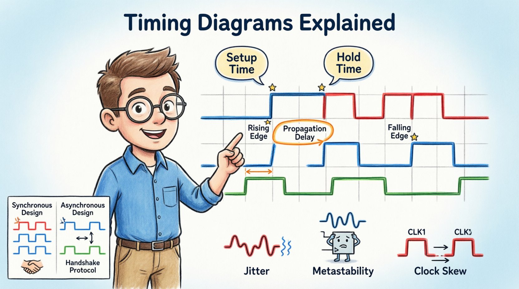
2. Setup Time (tsu)
Setup time is the minimum duration that data signals must be stable before a clock edge arrives.
- Scenario: If a flip-flop needs data to be ready 5 nanoseconds before the clock triggers, that is the setup time.
- Violation: If data changes too close to the clock edge, the system cannot capture the value correctly.
3. Hold Time (th)
Hold time is the minimum duration that data signals must remain stable after a clock edge arrives.
- Scenario: The flip-flop needs to “see” the data for a short period after the trigger to latch it securely.
- Violation: If data changes immediately after the clock edge, the input may not latch properly.
4. Clock Skew
Clock skew occurs when the clock signal arrives at different components at different times. This is often due to trace length differences on a PCB.
- Positive Skew: Clock arrives later at the destination.
- Negative Skew: Clock arrives earlier at the destination.
5. Jitter
Jitter is the short-term variation of a signal’s significant instants from their ideal positions in time. It adds uncertainty to the timing analysis.
📊 Comparison: Synchronous vs. Asynchronous Design
Understanding the difference between these two design philosophies is vital for interpreting timing diagrams correctly.
| Feature | Synchronous Timing | Asynchronous Timing |
|---|---|---|
| Control Signal | Uses a global clock | Uses handshaking signals |
| Predictability | Highly predictable | Variable based on load |
| Complexity | Requires clock distribution | Requires complex handshake logic |
| Power Consumption | Can be high (clock toggling) | Often lower (activity driven) |
| Timing Diagram | Aligned with clock edges | Dependent on previous state completion |
🧐 How to Read and Analyze Timing Diagrams
Analyzing a waveform requires a systematic approach. Follow these steps to ensure you do not miss critical details.
Step 1: Identify the Clock
Locate the primary clock signal. This is usually the reference for all other timing. In synchronous systems, every data transition should ideally be referenced to this clock edge.
Step 2: Check for Glitches
Look for short, unintended pulses (glitches) on signal lines. These can cause false triggers in logic gates. In a clean diagram, transitions should be clean, though real-world capture often shows noise.
Step 3: Verify Setup and Hold Windows
Draw imaginary vertical lines representing the setup and hold windows around the active clock edge. Ensure the data signal is stable within these zones.
Step 4: Check Control Signals
Ensure control signals like Chip Select (CS) or Enable (EN) are active for the entire duration of data transfer. If a control signal drops while data is still being sent, corruption occurs.
Step 5: Measure Intervals
Calculate the time between specific events. For example, measure the latency from a “Request” signal to the “Response” signal. This helps validate performance against specifications.
🚀 Advanced Concepts in Timing Analysis
As systems become faster and more complex, basic timing diagrams evolve into sophisticated analysis requirements.
1. Metastability
Metastability occurs when a flip-flop receives an input that violates setup or hold time requirements. Instead of resolving to a clear 0 or 1, the output enters an undefined state for an unpredictable duration.
- Cause: Often happens when asynchronous signals cross clock domains.
- Mitigation: Use synchronizer chains (multiple flip-flops in series) to reduce the probability of metastability.
- Visual: On a timing diagram, this looks like a signal oscillating or taking an abnormally long time to settle.
2. Setup and Hold Time Budgets
Engineers calculate a timing budget to ensure the system works at maximum frequency. This involves subtracting all delays (wire, gate, clock skew) from the clock period.
If the total delay exceeds the available time, the maximum operating frequency must be reduced.
3. High-Speed Interface Timing
Interfaces like DDR memory or PCIe require extremely precise timing. These diagrams often include:
- Eye Diagrams: A superposition of many signal transitions to visualize signal quality.
- Duty Cycle Distortion: Ensuring the High and Low times are balanced.
- Phase Alignment: Ensuring data and clock arrive in sync across multiple bits.
4. Power Management States
Modern devices enter low-power modes. Timing diagrams must account for the wake-up latency. For example, a signal asserting power to a peripheral must happen before the device is ready to receive data.
📝 Best Practices for Documentation
Clear documentation prevents errors during development and debugging. Adhere to these standards when creating or reviewing timing diagrams.
- Consistent Scaling: Use consistent time scales across related diagrams to allow easy comparison.
- Clear Labels: Every signal must be labeled with its function and logic polarity (e.g.,
RESET#for Active Low). - Zoom Levels: Provide both a high-level overview and a zoomed-in view of critical transitions (like setup/hold windows).
- Color Coding: Use colors to distinguish between different voltage domains or clock sources (e.g., Red for Clock, Blue for Data).
- Version Control: Timing requirements change. Ensure diagrams are versioned to match the hardware revision.
🛠️ Common Pitfalls and Troubleshooting
Even experienced engineers encounter timing issues. Here are common scenarios and how to address them.
Pitfall 1: Ignoring Trace Delay
PCB traces have physical length, which introduces delay. At high frequencies, a few inches of wire can equal a clock cycle.
- Solution: Account for trace length in your timing budget calculations.
Pitfall 2: Floating Inputs
Unconnected inputs can float to an intermediate voltage, causing oscillation.
- Solution: Ensure all inputs have defined pull-up or pull-down resistors.
Pitfall 3: Race Conditions
When two signals change simultaneously, the order of arrival determines the outcome.
- Solution: Use synchronization logic or state machines to sequence events.
Pitfall 4: Overshoot and Undershoot
Signal reflections can cause voltages to exceed power rails (overshoot) or drop below ground (undershoot).
- Solution: Implement proper termination resistors and impedance matching.
🔗 Real-World Applications
Timing diagrams are applied across various domains of engineering.
1. Memory Interfaces
DRAM and SDRAM require strict timing sequences for Read/Write operations. The CAS latency and RAS to CAS delay are critical parameters visualized in these diagrams.
2. Microcontroller Communication
Protocols like I2C, SPI, and UART rely on specific timing relationships between the clock and data lines. For example, in I2C, the data line must be stable while the clock is high.
3. Power Supply Sequencing
Complex systems require power rails to turn on in a specific order. Timing diagrams ensure that the core voltage is stable before the I/O voltage is applied.
🎯 Summary of Key Takeaways
Mastering timing diagrams requires patience and attention to detail. The following points summarize the essential knowledge for effective design and analysis.
- Time is Critical: Digital logic relies on precise temporal relationships between signals.
- Setup and Hold: These are the two most common constraints that dictate maximum operating speed.
- Visual Verification: Diagrams allow you to see potential conflicts before hardware is built.
- Context Matters: Always consider the physical environment (PCB, temperature, voltage) which affects signal timing.
- Standardization: Use standard symbols and notation to ensure communication clarity across teams.
By applying these principles, you ensure that your digital systems are robust, reliable, and performant. The ability to interpret and create these diagrams is a fundamental skill that separates functional designs from those that fail in the field.
📈 Moving Forward
As technology advances, timing constraints become tighter. Modern systems operate at gigahertz speeds where nanoseconds matter immensely. Continuous learning regarding signal integrity and timing closure is necessary for engineers working on cutting-edge hardware.
Start by analyzing existing schematics and their corresponding timing diagrams. Practice measuring intervals and identifying violations. Over time, the patterns will become intuitive, allowing you to predict issues before they manifest physically.