Understanding the behavior of digital circuits requires more than just knowing logic gates. It demands a grasp of how signals change over time. Timing diagrams provide the visual language for this temporal analysis. They map out the state of various signals relative to a clock or a specific event. For computer science students, mastering this concept is essential for designing reliable systems.
This guide explores the mechanics, reading techniques, and critical parameters involved in timing diagrams. We will cover everything from basic signal transitions to complex setup and hold time violations. By the end of this overview, you will have a solid foundation for analyzing digital interactions.
What is a Timing Diagram? ⏱️
A timing diagram is a graphical representation of the relationship between two or more signals over time. It acts as a timeline for digital events. Each signal is plotted as a horizontal line. The vertical position indicates the logic level or state. The horizontal axis represents the passage of time.
These diagrams are vital for verifying that a digital system operates correctly. They help engineers predict how data moves through registers, buses, and memory. Without them, debugging hardware issues becomes nearly impossible. They bridge the gap between abstract logic and physical reality.
Core Components of Digital Signals 📡
Before diving into the diagrams, one must understand the signals themselves. Digital systems rely on voltage levels to represent binary data. These levels are not always static; they transition between states.
- Logic High (1): Typically represents a voltage near the supply rail.
- Logic Low (0): Typically represents a voltage near ground.
- Edges: The transition points between high and low. Rising edges go from low to high. Falling edges go from high to low.
- Steady State: The period where a signal remains constant.
- Noise Margins: The tolerance a signal has before it is misinterpreted.
Timing diagrams visualize these transitions. They show exactly when a signal changes and how long it stays in that state. This precision is crucial for ensuring data integrity.
Understanding the Time Axis ⏳
The horizontal axis is the backbone of any timing diagram. It represents time progression. In digital design, this axis is often synchronized with a clock signal. The clock acts as the heartbeat of the system.
Units on the time axis vary based on the speed of the circuit. Common units include:
- Seconds (s): Used for very slow systems.
- Milliseconds (ms): 10^-3 seconds.
- Microseconds (µs): 10^-6 seconds.
- Nanoseconds (ns): 10^-9 seconds. Standard for modern processors.
- Picoseconds (ps): 10^-12 seconds. Required for high-speed interfaces.
When reading a diagram, look for the scale markers. They indicate the duration of each cycle. This helps in calculating propagation delays and ensuring signals arrive within the required window.
Synchronous vs Asynchronous Systems 🔄
Digital systems generally fall into two categories based on how they handle timing. Understanding the distinction is key to drawing accurate diagrams.
1. Synchronous Systems
In synchronous designs, all state changes occur relative to a global clock signal. The timing diagram will show a periodic clock waveform. Every flip-flop updates on the active edge of this clock.
- Advantages: Predictable behavior. Easier to verify.
- Challenges: Clock skew can cause issues if signals arrive at different times.
- Diagram Feature: Vertical lines often align with clock edges to show capture moments.
2. Asynchronous Systems
Asynchronous designs do not rely on a global clock. Instead, they use handshaking protocols or local signals to trigger actions. Timing diagrams here are more irregular.
- Advantages: Lower power consumption in some cases. Faster average response times.
- Challenges: Complex to verify. Prone to race conditions.
- Diagram Feature: Signals trigger each other without a fixed rhythm.
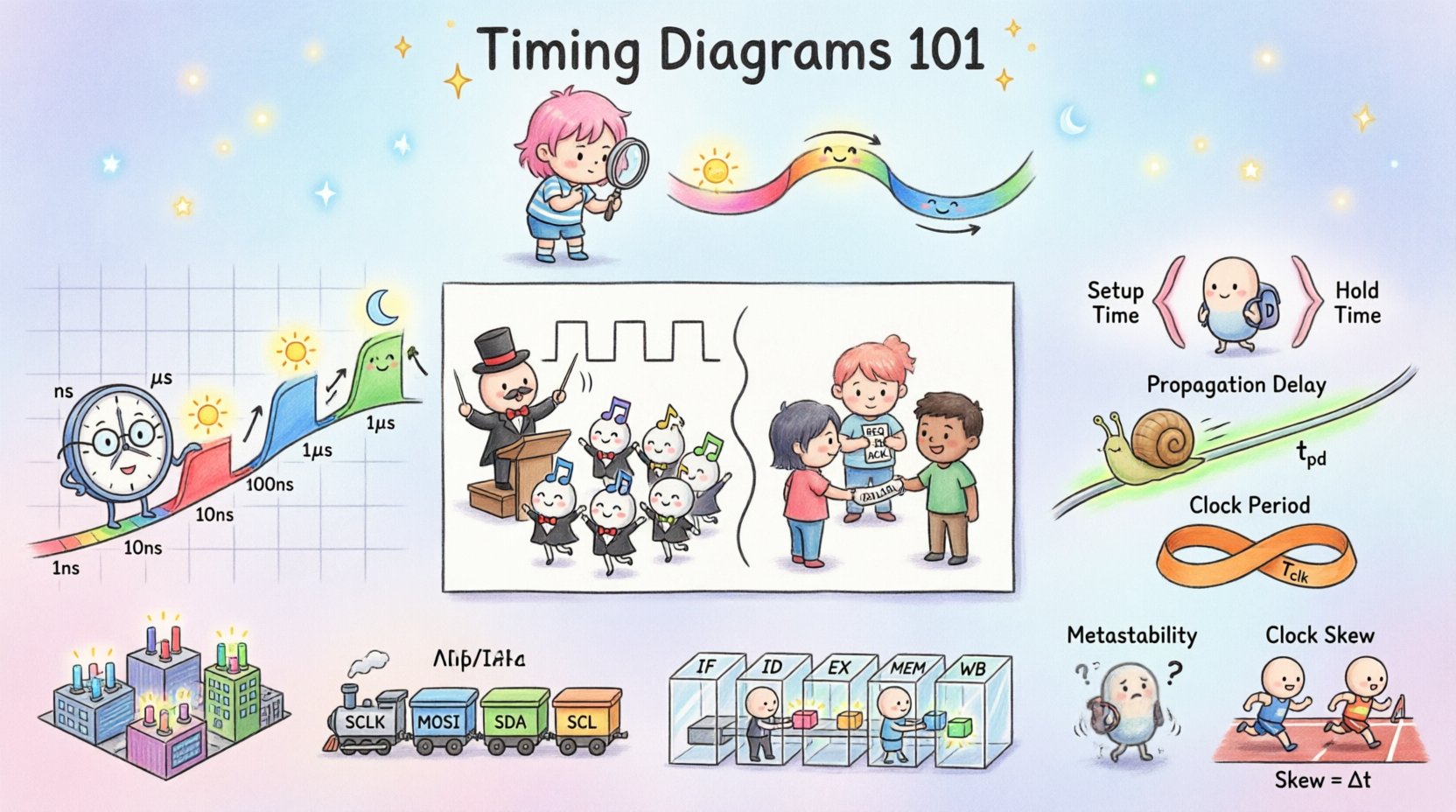
Critical Timing Parameters 📏
Specific measurements define the reliability of a timing diagram. These parameters determine whether a circuit will function correctly under all conditions.
| Parameter | Description | Significance |
|---|---|---|
| Propagation Delay | Time taken for a signal to travel from input to output. | Limits maximum operating frequency. |
| Setup Time | Time data must be stable before the clock edge. | Ensures the latch captures the correct value. |
| Hold Time | Time data must remain stable after the clock edge. | Prevents the latch from reading a changing value. |
| Clock Period | Duration of one complete cycle of the clock signal. | Defines the speed of the system. |
| Duty Cycle | Percentage of the period the signal is high. | Affects power consumption and timing margins. |
Deep Dive: Setup and Hold Times
Setup and hold times are the most critical constraints for sequential logic. If violated, the system may enter a metastable state where the output is undefined.
Setup Time Violation: This occurs when data changes too close to the clock edge. The circuit does not have enough time to prepare for the capture. The result is often a logic error.
Hold Time Violation: This occurs when data changes too soon after the clock edge. The circuit is still trying to capture the previous value. This is often harder to fix because it depends on the physical layout.
Reading and Analyzing Diagrams 🔍
Analyzing a timing diagram requires a systematic approach. Follow these steps to interpret the visual data accurately.
- Identify the Clock: Find the periodic signal. This is your reference point.
- Locate Active Edges: Determine if the system triggers on rising or falling edges.
- Trace Signal Dependencies: See how changes in one signal affect others.
- Check for Glitches: Look for short pulses that might be noise or unintended transitions.
- Verify Constraints: Ensure setup and hold times are respected for all registers.
Consider a simple data transfer scenario. A CPU sends data to memory. The timing diagram will show the address lines stabilizing first, followed by the data lines, and finally the write signal. Each step must happen within a specific window.
Common Violations and Their Impact ⚠️
Even experienced engineers encounter timing issues. Understanding common violations helps in troubleshooting.
1. Metastability
When a signal violates setup or hold time, the flip-flop output may oscillate before settling. This state is called metastability. It can propagate through the system, causing unpredictable behavior. Synchronization circuits are often used to mitigate this risk.
2. Skew
Clock skew happens when the clock signal arrives at different components at different times. This can reduce the effective timing margin. Positive skew gives more setup time but less hold time. Negative skew does the opposite.
3. Race Conditions
Race conditions occur when the output depends on the sequence of events. If two signals change simultaneously, the order of their processing determines the final state. Timing diagrams help visualize these sequences to prevent races.
Application in Computer Architecture 🖥️
Timing diagrams are not just theoretical tools. They are used extensively in real-world architecture.
Memory Interfaces
DRAM and SRAM have strict timing requirements. The memory controller must wait for specific delays before reading or writing. Timing diagrams define the command bus sequences. They ensure the memory bank is ready before data is accessed.
Bus Protocols
Protocols like I2C, SPI, and UART rely on timing for communication. The clock line in SPI synchronizes data transfer. In UART, the timing is based on baud rates. The receiver must sample the data line at the exact center of the bit period. A timing diagram shows the start bit, data bits, and stop bit alignment.
Pipeline Stages
Modern CPUs use pipelining to execute multiple instructions at once. Each stage must complete within one clock cycle. Timing diagrams map the flow of data through fetch, decode, execute, and write-back stages. They help identify stalls where one stage waits for another.
Best Practices for Documentation 📝
Creating clear timing diagrams ensures that other engineers can understand your design. Follow these guidelines for effective documentation.
- Use Consistent Scales: Ensure the time axis is uniform throughout the document.
- Label Clearly: Name every signal. Avoid generic labels like “Signal 1”.
- Highlight Constraints: Use brackets or shaded regions to show setup and hold windows.
- Group Related Signals: Keep control signals together and data signals together.
- Include Annotations: Add notes explaining complex transitions or special behaviors.
Advanced Considerations 🔬
As systems become faster, timing analysis becomes more complex. Several factors add layers of difficulty.
1. Power Supply Noise
Voltage fluctuations can shift the threshold levels of logic gates. This effectively changes the propagation delay. Timing diagrams must account for worst-case voltage scenarios.
2. Temperature Variations
Electronic components behave differently at different temperatures. High temperatures increase resistance and delay. Low temperatures can affect capacitance. Designers must verify timing across the full operating temperature range.
3. Signal Integrity
Long traces on a circuit board act as transmission lines. Reflections and crosstalk can distort signals. Timing diagrams should include eye diagrams or signal quality metrics for high-speed links.
Conclusion on Timing Analysis 🎯
Timing diagrams are the map for navigating digital logic. They translate abstract binary states into physical time events. For a computer science student, proficiency in reading and creating these diagrams is a core competency.
By understanding clock cycles, propagation delays, and setup constraints, you can design systems that are robust and efficient. The ability to visualize signal flow prevents costly errors in hardware design. As technology advances, the principles remain the same. Time is the constant variable.
Focus on the fundamentals. Practice reading existing diagrams. Draw your own for every new circuit you build. This discipline will serve you well in your technical career.