Digital systems rely on precise synchronization to function correctly. Without accurate timing, data corruption, system crashes, and safety failures become inevitable. A timing diagram provides a visual representation of how signals change over time, offering a clear view of the relationships between clock cycles, data validity, and control signals. This guide explores the critical role of timing diagrams across various sectors, detailing practical examples and technical solutions for common challenges.
🔍 Understanding the Fundamentals
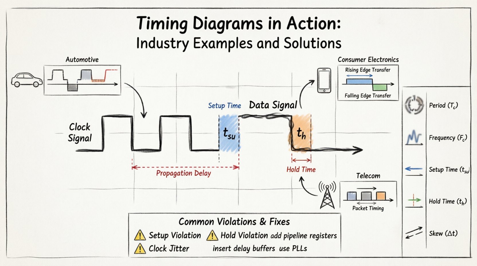
Before diving into specific applications, it is essential to grasp the core components of a timing diagram. These diagrams map the behavior of signals relative to a reference clock. They are not merely drawings; they are mathematical constraints that dictate hardware behavior.
- Signal Edges: The transition from low to high (rising edge) or high to low (falling edge) triggers state changes in sequential logic.
- Clock Period: The duration between two consecutive edges of the same polarity defines the available time for logic to settle.
- Propagation Delay: The time it takes for a signal to travel from an input pin to an output pin through logic gates.
- Setup and Hold Times: Critical constraints ensuring data is stable before and after the clock edge.
When these parameters are violated, the circuit may enter a metastable state, leading to unpredictable behavior. Engineers use timing diagrams to verify that the physical implementation of a design adheres to these logical requirements.
🚗 Automotive Electronics: Safety-Critical Timing
The automotive industry demands the highest level of reliability. Vehicles contain dozens of Electronic Control Units (ECUs) communicating over buses like CAN (Controller Area Network), LIN (Local Interconnect Network), and FlexRay. Timing analysis here is not just about speed; it is about determinism and safety.
1. CAN Bus Arbitration
CAN bus allows multiple nodes to communicate on a single wire. The timing diagram for CAN arbitration reveals how priority is determined during bus contention.
- Dominant vs. Recessive: Logic levels are represented by voltage states. A dominant bit (0) overrides a recessive bit (1).
- Synchronization: Nodes synchronize to the start of frame bit using synchronization segments.
- Sampling Point: Data is sampled at a specific percentage of the bit time to avoid noise.
If the sampling point is too close to the edge, noise can cause bit errors. If it is too late, the data may not be stable. Timing diagrams help engineers set the sampling point correctly, typically around 80% of the bit time.
2. ADC Sampling in Sensor Fusion
Modern vehicles use multiple sensors (radar, lidar, cameras) to create a perception of the environment. Analog-to-Digital Converters (ADCs) must sample signals at precise intervals to avoid aliasing.
- Clock Jitter: Variations in the clock edge timing introduce noise into the digitized signal.
- Latency: The time from sensor input to processed data output must be minimized for real-time control.
- Interleaving: Multiple ADCs often work in parallel. Timing diagrams ensure their phases are aligned to prevent gaps in data.
📱 Consumer Electronics: High-Speed Interfaces
Consumer devices prioritize performance and power efficiency. Interfaces like DDR memory and display links require tight timing windows to achieve high bandwidth without increasing power consumption.
1. DDR Memory Interfaces
Double Data Rate (DDR) memory transfers data on both the rising and falling edges of the clock. This doubles the effective data rate but halves the time window for data stability.
| Parameter | Definition | Impact of Violation |
|---|---|---|
| Setup Time | Time data must be stable before the clock edge | Missed data transfer, system hang |
| Hold Time | Time data must remain stable after the clock edge | Corrupted data, bit flips |
| Clock Skew | Difference in arrival time of clock to different chips | Reduced timing margin, instability |
| Duty Cycle | Ratio of high time to total period | Unbalanced performance, increased jitter |
In DDR4 and DDR5, the command and address bus often run at a lower frequency than the data bus. Timing diagrams must account for the source-synchronous strobe signals (DQS) that accompany the data to indicate valid windows.
2. Display Interfaces (MIPI DSI)
Mobile devices use the MIPI Display Serial Interface (DSI) to connect the processor to the screen. This interface uses high-speed differential lanes.
- LP Command Mode: Low power mode for sending commands, relying on strict timing for wake-up sequences.
- HS Data Mode: High-speed transmission where clock recovery is performed on the data stream.
- Turnaround Time: The time required to switch from transmit to receive mode on the same lane.
Misalignment in these timing diagrams results in screen artifacts, flickering, or a complete loss of video output.
📡 Telecommunications: Latency and Bandwidth
In telecommunications, timing is synonymous with latency. Packet delivery times and synchronization across distributed networks are critical for services like 5G and high-frequency trading.
1. PCIe Signaling
The Peripheral Component Interconnect Express (PCIe) standard is widely used for connecting high-speed components. It uses serial lanes with embedded clocks or source-synchronous clocks.
- Equalization: Signal integrity degrades over distance. Timing diagrams show how equalization filters compensate for loss.
- Link Training: A sequence of timed states to establish the link speed and lane width.
- Flow Control: Timing windows for credit-based flow control prevent buffer overflows.
2. Ethernet PHYs
Standard Ethernet relies on a shared clock or clock recovery. Gigabit Ethernet and beyond use 8b/10b encoding to ensure sufficient transitions for clock recovery.
- Idle Periods: Defined timing windows where no data is sent to maintain synchronization.
- Start of Frame Delimiter: A specific bit pattern that marks the beginning of a packet, requiring precise detection timing.
- Inter-Packet Gap: A mandatory delay between packets to allow hardware to reset.
⚠️ Common Timing Violations and Solutions
Even with careful design, timing violations occur. Identifying the root cause requires analyzing the timing diagram to see where signals diverge from expectations.
1. Setup Time Violations
Occurs when data arrives too late to be captured by the clock edge.
- Causes: Excessive logic depth, long wire delays, or clock skew.
- Solutions:
- Insert pipeline registers to break long paths.
- Optimize logic synthesis to reduce gate count.
- Adjust clock frequency to provide more time.
2. Hold Time Violations
Occurs when data changes too quickly after the clock edge, overwriting the captured value.
- Causes: Short path delays, clock skew where the capture clock arrives too late.
- Solutions:
- Insert delay buffers in the data path.
- Use retiming techniques to balance paths.
- Ensure clock distribution network has minimal skew.
3. Clock Skew and Jitter
Skew is the difference in arrival time of the clock signal at different registers. Jitter is the short-term variation of the clock edge.
- Impact: Reduces the effective timing margin available for data.
- Solutions:
- Use low-jitter clock generators.
- Design balanced clock trees with equal length traces.
- Implement Phase-Locked Loops (PLLs) to clean up clock signals.
✅ Best Practices for Implementation
Achieving robust timing requires a systematic approach throughout the design lifecycle. Documentation and verification are as important as the circuit itself.
1. Define Timing Constraints Early
Do not wait until the implementation phase to define timing requirements. Document the clock frequencies, input delays, and output delays in the design specification. This ensures all stakeholders understand the boundaries of the system.
2. Use Static Timing Analysis
Static Timing Analysis (STA) tools calculate the worst-case delay paths without simulating every input combination. This method is efficient and covers all possible states, ensuring no timing violations are missed.
3. Validate with Simulation
While STA is powerful, dynamic simulation provides a view of signal behavior under specific conditions. Use simulation to verify critical paths, especially those involving asynchronous logic or complex state machines.
4. Physical Design Considerations
The physical layout of the chip or board directly impacts timing.
- Wire Length: Longer wires introduce more capacitance and resistance, increasing delay.
- Crosstalk: Neighboring signals can induce noise, causing false transitions.
- Power Supply Noise: Voltage drops can slow down gate switching speeds.
🛠️ Troubleshooting Real-World Scenarios
When a system fails to meet timing, a structured debugging process is necessary. The following steps outline a logical approach to resolving timing issues.
- Step 1: Identify the Path. Locate the specific register-to-register path causing the failure. Look at the timing report for the most negative slack.
- Step 2: Analyze the Waveforms. Use a timing diagram viewer to inspect the actual signal transitions. Compare them against the expected values.
- Step 3: Check the Clock. Verify the clock signal quality. Look for jitter, duty cycle distortion, or glitches.
- Step 4: Review Constraints. Ensure the constraints in the design file match the physical reality of the hardware.
- Step 5: Iterate. Make changes to the logic or layout, then re-run the timing analysis.
📊 Summary of Timing Parameters
To aid in quick reference, here is a summary of key timing parameters used across industries.
| Parameter | Symbol | Typical Unit | Description |
|---|---|---|---|
| Period | Tc | ns | Time between consecutive clock edges |
| Frequency | Fc | Hz | Inverse of the period |
| Setup Time | tsu | ns | Data stability required before clock edge |
| Hold Time | th | ns | Data stability required after clock edge |
| Propagation Delay | tpd | ns | Time for signal to pass through logic |
| Skew | Δt | ps | Clock arrival time difference |
🔄 Managing Asynchronous Designs
Not all systems run on a single clock. Asynchronous designs involve data crossing between different clock domains. This introduces the risk of metastability, where a flip-flop enters an undefined state.
- Synchronization Chains: Use a multi-stage synchronizer (typically two flip-flops) to allow the signal to settle before being used.
- Handshake Protocols: Implement request-acknowledge mechanisms to ensure the receiver is ready before data is sent.
- FIFO Buffers: Use First-In-First-Out memory structures to decouple the producer and consumer speeds.
Timing diagrams for asynchronous designs show the relationship between the two independent clocks. The key is to ensure that the data path has enough time to stabilize before the receiving clock samples it.
🌟 Final Thoughts
Timing diagrams are the backbone of digital system verification. They bridge the gap between abstract logic and physical reality. By understanding the nuances of setup time, hold time, clock skew, and jitter, engineers can design systems that are robust, efficient, and reliable.
Whether in automotive safety systems, consumer gadgets, or telecommunications infrastructure, the principles remain the same. Precision in timing leads to precision in performance. Continuous monitoring and adherence to best practices ensure that designs remain functional throughout their lifecycle. As technology advances and speeds increase, the importance of detailed timing analysis will only grow.
For teams looking to improve their design quality, investing time in accurate timing diagrams and verification flows is essential. It reduces risk, lowers debugging costs, and ensures that the final product meets its specifications. With the right tools and methodologies, timing challenges become manageable constraints rather than obstacles.