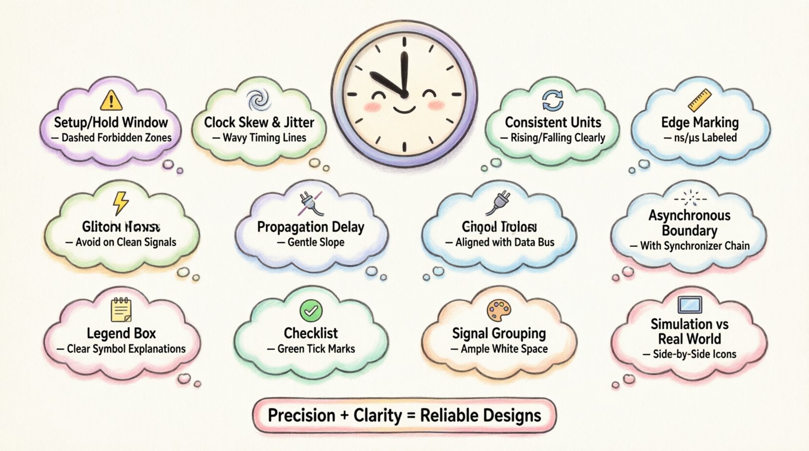
Timing diagrams are the backbone of digital system verification. They translate abstract logic into visual timelines that engineers, designers, and testers rely on to validate signal behavior. When a timing diagram contains errors, the consequences extend far beyond the drawing board. Incorrect timing assumptions can lead to hardware failures, data corruption, or system instability in production environments. This guide explores the most frequent pitfalls found in timing analysis and provides concrete strategies to ensure accuracy.
Creating a precise timing diagram requires more than just drawing lines. It demands a deep understanding of clock domains, signal propagation, and physical constraints. Engineers often rush through the visualization phase, overlooking subtle details that become critical during implementation. By recognizing these common mistakes early, teams can save significant time during debugging and integration phases. Let us examine the specific areas where errors typically occur.
1. Misinterpreting Setup and Hold Time Violations ⚠️
Setup and hold times are fundamental constraints in synchronous digital design. A setup violation occurs when data arrives too late before the active clock edge. A hold violation happens when data changes too soon after the clock edge. These are not just theoretical concepts; they represent physical limits of flip-flops and logic gates.
Many diagrams fail to clearly indicate the window of validity for data signals. When drawing these signals, engineers sometimes omit the critical setup and hold windows, leading to ambiguity during review. A robust diagram should explicitly mark these windows relative to the clock edge.
- Common Error: Drawing data transitions aligned exactly with the clock edge without considering jitter or skew.
- Common Error: Ignoring the direction of the edge (rising vs. falling) for setup/hold windows.
- Common Error: Assuming ideal clock edges with zero transition time.
To avoid these issues, always annotate the setup and hold margins. Use distinct shading or markers to show the forbidden zones where data transitions are invalid. This visual cue forces reviewers to check if the signal path complies with the timing requirements of the receiving logic.
2. Neglecting Clock Skew and Jitter 🌪️
Clock skew refers to the difference in arrival times of the clock signal at different components. Jitter represents the short-term variations in the clock signal’s timing. Both factors can drastically alter the effective timing windows for data signals.
A common mistake in diagrams is treating the clock as a perfectly straight vertical line across all components. In reality, distribution networks introduce delays. If a diagram shows a single clock line branching out to three different registers without accounting for path differences, it presents an unrealistic view of the system behavior.
- Impact: Skew can reduce the available time for data to propagate, causing false setup violations.
- Impact: Jitter can shrink the hold time margin, increasing the risk of metastability.
When creating diagrams, represent clock paths as separate lines with relative offsets if the skew is significant. If the skew is negligible, state that assumption clearly in the diagram notes. Do not hide the clock distribution complexity if it affects the timing budget.
3. Inconsistent Time Scales and Units 📏
One of the simplest yet most damaging errors is mixing time scales within a single diagram. A section might show nanoseconds while another shows microseconds. This inconsistency forces the reader to constantly recalculate ratios, increasing the chance of misinterpretation.
Another issue is the lack of a clear time axis. Without a scale bar or labeled ticks, the duration of pulses becomes subjective. A short pulse might be 10 nanoseconds or 100 nanoseconds depending on how the reader interprets the spacing.
Follow these standards to maintain consistency:
- Define the Scale: Place a time ruler at the bottom or top of the diagram.
- Use Scientific Notation: Clearly label units (ns, μs, ps) in the header.
- Keep Ratios Proportional: Ensure the horizontal distance between events matches the time difference.
Consistency builds trust. When every engineer looks at the diagram, they should derive the same timing values without needing to make assumptions about the drawing scale.
4. Ambiguity in Edge Triggers 🔄
Digital logic often relies on specific edge triggers, such as rising edge or falling edge. A timing diagram must explicitly show which edge triggers the action. Ambiguity here can lead to completely opposite behavior in the hardware.
A common mistake is drawing a clock signal without indicating the active edge. For example, if a flip-flop triggers on the falling edge but the diagram looks identical to a rising edge trigger, the logic designer might implement the wrong behavior.
- Best Practice: Use arrows on the clock line to indicate the active edge.
- Best Practice: Label the trigger type in the legend (e.g., “Posedge”, “Nedge”).
- Best Practice: Avoid using double arrows unless both edges are active.
Clarity is paramount. If a signal is asynchronous, ensure it is clearly separated from the clock domain to avoid confusion about which edge controls it.
5. Overlooking Propagation Delays ⏳
Propagation delay is the time it takes for a signal to travel from input to output through a logic gate or wire. In ideal diagrams, signals appear to change instantly. In physical systems, there is always a delay.
When designers omit propagation delays, the timing diagram suggests that the output changes immediately after the input changes. This can mask timing violations that will occur in silicon. For instance, a combinational path might appear to meet the clock period in the diagram, but the actual delay pushes the data past the next clock edge.
| Feature | Ideal Diagram | Real-World Implementation |
|---|---|---|
| Signal Transition | Vertical Line | Sloped Line with Delay |
| Propagation | Instantaneous | Gate Delay + Wire Delay |
| Setup Margin | Often Unchecked | Must Account for Worst Case |
To mitigate this, annotate the expected delay for critical paths. If the delay is significant relative to the clock period, draw the transition with a slope or explicitly mark the delay value. This visual representation helps reviewers spot potential bottlenecks before fabrication.
6. Ignoring Metastability Risks 🌌
Metastability occurs when a flip-flop receives data near the clock edge, causing it to enter an undefined state for an unpredictable duration. Timing diagrams rarely capture this state explicitly because it is a failure mode, not a normal operation.
However, ignoring the possibility of metastability in asynchronous interfaces is a critical oversight. If a diagram shows an asynchronous signal synchronizing to a clock without a synchronizer chain, it implies a risk of data loss or corruption.
- Identification: Look for signals crossing clock domains without proper synchronization.
- Documentation: Note where metastability is a known risk and how it is mitigated.
- Visualization: Use dashed lines to indicate asynchronous boundaries.
Even if the system is designed to handle metastability, the diagram should reflect the synchronization stages. This ensures that the verification team knows to test for these specific conditions.
7. Signal Glitches and Hazards ⚡
Glitches are transient pulses that occur due to unequal propagation delays in parallel paths. They can cause false triggering of logic if not accounted for in the timing analysis.
A common mistake is drawing clean, steady signals where glitches are physically inevitable. For example, in a multiplexer switching between inputs, the output might briefly flicker before settling. If the diagram shows a smooth transition, the downstream logic might not be designed to filter these glitches.
Highlight potential hazard zones in the diagram. Use annotations to warn that a specific signal may exhibit transient behavior during state changes. This informs the testing strategy to include glitch detection scenarios.
8. Lack of Context for Control Signals 🔌
Data signals are useless without the context of control signals like enable, reset, or chip select. A diagram that focuses solely on data lines often misses the conditions required for that data to be valid.
For example, a data bus might show valid values, but if the “Write Enable” signal is not shown as active during that window, the data is effectively ignored. Conversely, if the “Write Enable” is active but the data is invalid, the system writes garbage.
- Include Control: Always display control signals alongside data signals.
- Define Validity: Use a “Valid” flag or similar indicator to denote when data is reliable.
- State Conditions: Clearly label the state of control signals (High Active vs. Low Active).
Completeness is key. A timing diagram that lacks control signal context is often a source of confusion during debugging. Ensure the relationship between control and data is visually explicit.
9. Poor Annotation and Legend Usage 📝
Even a perfectly accurate diagram can be misunderstood if it lacks proper annotations. Symbols, abbreviations, and legends must be consistent and explained.
Common annotation errors include:
- Using generic labels like “Signal A” instead of descriptive names.
- Failing to explain the meaning of specific line styles (solid vs. dashed).
- Omitting the active level definition (Active High vs. Active Low).
A dedicated legend section should be part of every timing diagram. It defines every symbol, line style, and abbreviation used. This reduces the cognitive load on the reader and ensures everyone interprets the diagram the same way.
10. Verification and Review Checklist ✅
Before finalizing a timing diagram, a systematic review is necessary. Use the following checklist to validate the accuracy and clarity of your work.
| Check Item | Pass Criteria |
|---|---|
| Time Scale | Consistent units and clear ruler provided |
| Clock Edge | Active edge clearly marked for all clocks |
| Setup/Hold | Windows defined for synchronous signals |
| Propagation | Delays accounted for in critical paths |
| Control Signals | Enable/Reset signals shown with data |
| Legends | All symbols and abbreviations explained |
| Domain Crossing | CDC points identified and marked |
Regularly updating this checklist ensures that no common mistake slips through the cracks. It serves as a quality gate for documentation before it reaches the engineering team.
11. Visual Clarity and Layout Design 🎨
The layout of a timing diagram affects how easily errors are detected. Crowded diagrams with overlapping signals are prone to misreading. Vertical alignment of related signals helps the eye trace the relationship between events.
Follow these layout principles:
- Group Signals: Keep related signals (like address and data) close together.
- Align Edges: Ensure clock edges are vertically aligned across all channels.
- Space Out: Leave enough white space to avoid signal overlap.
- Color Coding: Use different colors for different clock domains if available (though black and white is standard for print).
A clean layout reduces the cognitive effort required to interpret the diagram. This makes it easier to spot anomalies and timing violations at a glance.
12. Real-World Constraints vs. Simulation 🖥️
Timing diagrams derived purely from simulation might not reflect physical realities. Simulation tools often assume ideal conditions, such as zero parasitic capacitance and perfect routing.
When translating simulation results to documentation, engineers must account for manufacturing variations. Process, Voltage, and Temperature (PVT) corners can shift timing margins. A diagram that only shows nominal values might be insufficient for robust design.
- Worst Case: Consider the slowest process corner for timing analysis.
- Fastest Case: Consider the fastest process corner for hold time analysis.
- Margin: Add safety margins to the diagram to account for PVT variations.
Documentation should reflect the robustness of the design, not just the best-case simulation results. This prepares the team for real-world deployment scenarios.
Final Thoughts on Timing Accuracy 🛡️
Timing diagrams are communication tools as much as they are technical specifications. Their primary goal is to convey intent and constraints clearly to all stakeholders. By avoiding common mistakes such as neglecting skew, ignoring edge triggers, or omitting control signals, engineers ensure that the design intent is preserved from documentation to hardware.
Accuracy in these diagrams prevents costly re-spins and debugging cycles. A well-structured diagram serves as a single source of truth for the entire project lifecycle. Invest the time to get the timing analysis right, and the downstream implementation will follow smoothly.
Remember that a timing diagram is a living document. It should be updated whenever the design changes. Maintaining the integrity of the timing information ensures that the system remains reliable throughout its operational life. Focus on precision, clarity, and completeness to deliver robust digital designs.