In digital electronics and computer engineering, understanding the temporal relationship between signals is fundamental to system reliability. A timing diagram serves as the primary visual language for describing these relationships. It maps signal states against a time axis, allowing engineers to visualize data flow, clock synchronization, and potential hazards within a circuit. This guide explores the structural elements, operational patterns, and critical scenarios found in waveform analysis.
Whether designing integrated circuits or debugging embedded systems, the ability to interpret and create accurate timing representations is a core competency. This document provides a technical overview of how signals interact, the constraints they must satisfy, and the common pitfalls encountered during verification.
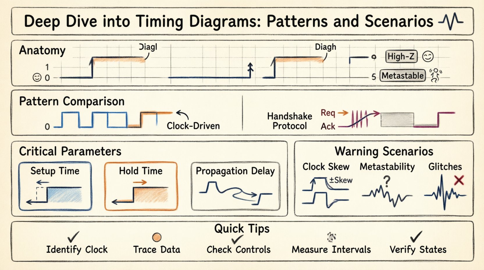
📐 Anatomy of a Timing Diagram
A timing diagram is a graphical representation where the horizontal axis represents time, and the vertical axis represents signal levels. Each horizontal line corresponds to a specific signal or net within the design. Understanding the components is the first step toward accurate analysis.
- Time Axis: Usually runs horizontally from left to right. It may be linear or logarithmic, depending on the scale of events being observed.
- Signal Lines: Individual traces representing voltage levels. High voltage typically denotes logic 1, while low voltage denotes logic 0.
- Transitions: Vertical lines indicating a change in state, such as a rising edge (0 to 1) or falling edge (1 to 0).
- Labels: Text annotations identifying specific signals, pins, or control lines.
- Markers: Vertical dashed lines often used to denote specific events, such as a clock pulse or a reset trigger.
🔢 Logic Levels and States
Digital signals do not always exist strictly at 0 or 1. In practical scenarios, signals can exist in undefined states or high-impedance states. A complete diagram should account for these variations.
- Logic High (1): The signal is driven to a voltage level recognized as a logical true.
- Logic Low (0): The signal is driven to a voltage level recognized as a logical false.
- High-Z: The signal is disconnected from the driver, effectively floating. This is common in tri-state buffers.
- Metastable: A state where the signal is neither high nor low, often occurring during asynchronous transitions.
⚙️ Common Timing Patterns
Designs follow predictable patterns to ensure data integrity. These patterns define how data moves relative to control signals. Recognizing these patterns helps in verifying that a design meets its specifications.
📌 Synchronous Data Transfer
Synchronous designs rely on a global clock signal to coordinate actions. Data is sampled only at specific moments, typically the rising or falling edge of the clock.
- Clock Driven: All state changes occur in relation to the clock edge.
- Data Validity: Data must be stable before the clock edge and remain stable after it.
- Propagation: There is a delay between the clock edge and when the output changes.
📌 Asynchronous Handshaking
Asynchronous communication does not rely on a shared clock. Instead, it uses control signals to indicate when data is ready and when it has been received.
- Request (Req): The sender signals that data is available.
- Acknowledge (Ack): The receiver signals that data has been accepted.
- Wait States: The sender may pause until the receiver is ready.
| Feature | Synchronous Pattern | Asynchronous Pattern |
|---|---|---|
| Coordination | Global Clock Signal | Control Handshake Signals |
| Speed | Generally Higher | Variable, dependent on response |
| Complexity | Clock Distribution Network | Protocol Logic |
| Latency | Predictable | Variable |
⏱️ Critical Timing Parameters
Beyond the visual lines, specific numerical constraints define whether a circuit will function correctly. These parameters are critical for static timing analysis and must be verified against physical limits.
🛑 Setup Time
Setup time is the minimum amount of time the data signal should be held stable before the clock edge. If data changes too close to the clock edge, the receiving flip-flop may not capture the correct value.
- Measurement: Measured from the active clock edge backward in time.
- Risk: Violation leads to incorrect data capture.
- Requirement: Data path delay must be long enough to meet the setup window.
🛑 Hold Time
Hold time is the minimum amount of time the data signal should be held stable after the clock edge. This ensures the latch has enough time to lock the input value.
- Measurement: Measured from the active clock edge forward in time.
- Risk: Violation leads to metastability or capture of wrong data.
- Requirement: Data path delay must be short enough to allow the hold time window.
⚡ Propagation Delay
This is the time it takes for a signal to travel from the input of a logic gate to its output. It varies based on the load capacitance and the internal resistance of the transistor.
- tpd (High to Low): Time to transition from 1 to 0.
- tpd (Low to High): Time to transition from 0 to 1.
- Skew: Differences in delay between parallel paths.
🚨 Critical Timing Scenarios
Certain scenarios present significant challenges that require careful analysis. These situations often involve interactions between different clock domains or physical limitations of the hardware.
🔄 Clock Skew
Clock skew occurs when the clock signal arrives at different components at different times. This can happen due to routing differences or physical distance.
- Positive Skew: The destination clock arrives later than the source clock.
- Negative Skew: The destination clock arrives earlier than the source clock.
- Impact: Can effectively reduce setup time margins or increase hold time violations.
🌊 Metastability
Metastability is a state where a flip-flop output is neither high nor low. It usually occurs when setup or hold times are violated, particularly in asynchronous crossings.
- Resolution: The circuit eventually resolves to a stable state, but the time taken is unpredictable.
- Fix: Use synchronizers (multi-stage flip-flops) to reduce the probability of failure.
- MTBF: Mean Time Between Failures is calculated based on metastability resolution rates.
📉 Glitches
Glitches are short-lived spikes in the signal that can be mistaken for valid transitions. They often occur due to differences in propagation delays along different paths.
- Causes: Unequal path lengths or race conditions.
- Effect: Can trigger unintended state changes in downstream logic.
- Mitigation: Use filtering logic or ensure proper timing closure.
🔍 Analyzing Waveforms
When reviewing a timing diagram, a systematic approach ensures no detail is overlooked. Engineers must trace the flow of data and control signals to identify discrepancies.
🔍 Step-by-Step Analysis
- Identify the Clock: Locate the primary clock signal. Determine if it is rising-edge or falling-edge triggered.
- Trace Data Paths: Follow the data lines from the source to the destination.
- Check Control Signals: Verify that enables, resets, and clears are asserted correctly.
- Measure Intervals: Calculate the time between specific events to verify setup and hold requirements.
- Verify State Transitions: Ensure the output state matches the expected logic function.
🔍 Reading Edge Triggers
Understanding how a component reacts to signal edges is vital.
- Positive Edge Triggered: The action occurs at the transition from low to high.
- Negative Edge Triggered: The action occurs at the transition from high to low.
- Level Triggered: The action occurs as long as the signal remains at a specific level.
🛠️ Documentation Standards
Clear documentation ensures that designs are understood by other engineers. Consistency in notation and labeling prevents misinterpretation during debugging or handoff.
📝 Labeling Conventions
- Signal Names: Use consistent naming conventions (e.g.,
clk,rst_n,data_in). - Polarity: Indicate active-low signals clearly, often with a bar or suffix.
- Units: Clearly state time units (ns, µs, ms) on the time axis.
- Scaling: Ensure the time scale is appropriate for the events shown.
📝 Visual Clarity
- Spacing: Avoid overlapping lines where possible.
- Contrast: Use distinct colors or line weights for different signal types.
- Annotations: Add notes explaining complex behaviors or specific constraints.
- Grid: Use a grid background to assist in measuring time intervals.
🚧 Troubleshooting Workflow
When a design fails to meet timing requirements, a structured troubleshooting process helps isolate the root cause. This involves examining the diagram against the physical constraints.
🚧 Identifying Violations
- Check Setup Time: Is the data arriving too late relative to the clock?
- Check Hold Time: Is the data changing too soon after the clock?
- Check Clock Frequency: Is the clock period shorter than the required minimum?
🚧 Mitigation Strategies
- Pipeline Registers: Insert additional registers to break long combinational paths.
- Clock Gating: Reduce activity to lower power and potentially improve timing.
- Buffer Insertion: Add buffers to balance delays across parallel paths.
- Timing Constraints: Define false paths to exclude logic that does not affect data flow.
📈 Best Practices for Design
Adopting best practices during the design phase reduces the likelihood of timing issues later in the development cycle. Proactive planning is more efficient than reactive fixing.
- Standardize Interfaces: Use known protocols for data transfer to simplify timing verification.
- Minimize Asynchronous Paths: Keep asynchronous interactions to a minimum to reduce metastability risks.
- Document Assumptions: Clearly state clock frequencies and voltage levels in the design specs.
- Review Regularly: Conduct timing reviews at every major milestone of the project.
🎯 Summary of Key Concepts
Timing diagrams are essential tools for visualizing the temporal behavior of digital systems. They reveal how data and control signals interact over time, highlighting critical constraints like setup and hold times. By understanding the anatomy of these diagrams, engineers can identify patterns, predict errors, and ensure robust system performance.
Key takeaways include the distinction between synchronous and asynchronous patterns, the importance of clock skew management, and the need for clear documentation standards. Adhering to these principles facilitates reliable design and simplifies the verification process.
Continuous analysis of waveform data ensures that designs remain within operational limits. As technology advances and clock speeds increase, the precision required in timing analysis becomes even more critical. Mastery of these concepts allows for the creation of stable, high-performance digital architectures.