In the world of digital electronics and hardware engineering, the communication between components relies on precise coordination. Without a clear understanding of when signals change state, systems fail. The timing diagram serves as the blueprint for this coordination. It visualizes the relationship between signals over time, revealing whether data is valid, stable, and ready for processing. This guide addresses the fundamental questions engineers and students face when analyzing these critical visual tools.
Whether you are designing a microcontroller interface, debugging a communication protocol, or studying digital logic, understanding the temporal aspects of your design is non-negotiable. This article explores the anatomy of timing diagrams, explains key parameters, and answers common questions regarding signal integrity and synchronization.
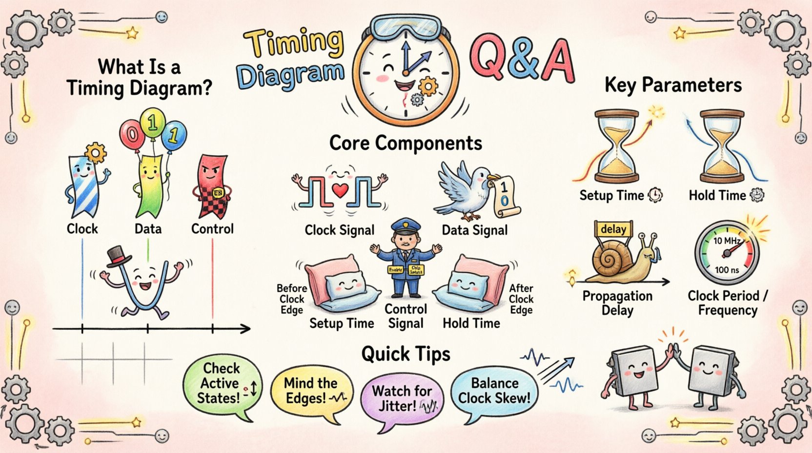
What Exactly Is a Timing Diagram? 📊
A timing diagram is a graphical representation of the sequence of events in a system. It plots signal levels against a horizontal time axis. Unlike a logic diagram, which shows connectivity, a timing diagram shows behavior. It allows you to see if a signal transitions high or low before or after another signal. This visual context is essential for verifying that a receiver has enough time to read data before the next clock edge arrives.
Key characteristics include:
- Time Axis: Usually runs horizontally from left to right.
- Signal Lines: Horizontal lines representing individual wires or data buses.
- Logic Levels: High (1) and Low (0) states are depicted as distinct voltage plateaus.
- Edges: Vertical lines indicating the transition from one state to another.
Core Components of a Timing Diagram 🧩
To read these diagrams effectively, you must identify the standard elements that make up the waveform. Each element plays a specific role in the synchronization of the system.
| Component | Description | Visual Indicator |
|---|---|---|
| Clock Signal | Provides the heartbeat for the system. Other signals are often sampled relative to this. | Regular square wave pattern |
| Data Signal | Carries the actual information being transferred. | Irregular transitions based on input |
| Control Signal | Manages the flow of data (e.g., Enable, Chip Select, Write). | Active high or active low pulses |
| Setup Time | The duration data must be stable before a clock edge. | Horizontal distance before the edge |
| Hold Time | The duration data must remain stable after a clock edge. | Horizontal distance after the edge |
Understanding Key Timing Parameters ⚙️
Timing parameters define the constraints within which a digital circuit operates correctly. Violating these parameters often leads to unpredictable behavior. Below are the definitions and implications of the most critical metrics.
1. Setup Time ⏳
Setup time is the minimum amount of time the data signal should be held stable before the triggering edge of the clock signal. If the data changes too close to the clock edge, the flip-flop may not capture the value correctly. This is often the most critical constraint in high-speed designs because it dictates the maximum frequency of operation.
2. Hold Time ⏳
Hold time is the minimum amount of time the data signal should be held stable after the triggering edge of the clock signal. Unlike setup time, hold time is generally independent of the clock frequency. It depends on the internal delay of the flip-flop and the external propagation delay of the data path.
3. Propagation Delay ⏳
This is the time it takes for a signal to travel from the input of a component to its output. It varies based on temperature, voltage, and manufacturing tolerances. In a timing diagram, this appears as the lag between a change in one signal and the resulting change in another.
4. Clock Period and Frequency ⏳
The clock period is the duration of one complete cycle of the clock signal. Frequency is the inverse of the period. A shorter period means a higher frequency, which allows for faster processing but tightens the window for signal stability.
Frequently Asked Questions ❓
Engineers often encounter specific scenarios that cause confusion. Here are detailed answers to the most pressing questions regarding timing analysis.
Q: What happens if setup time is violated? 🛑
When the setup time requirement is not met, the flip-flop enters a state known as metastability. In this state, the output does not settle immediately to a valid logic high or low. Instead, it may oscillate or remain at an intermediate voltage level for an unpredictable amount of time. This can cause the downstream logic to read a corrupted value, leading to system errors or crashes. In severe cases, metastability can propagate through the entire circuit, causing a functional failure that is difficult to debug.
Q: How do I handle clock skew? 🔄
Clock skew occurs when the clock signal arrives at different components at different times. This can happen due to varying path lengths or loading differences. To manage skew:
- Balance Routing: Ensure clock traces are routed with similar lengths and widths.
- Buffering: Use clock buffers to drive multiple loads evenly.
- Timing Margins: Design the system with enough slack in setup and hold times to absorb minor skew variations.
Q: What is the difference between synchronous and asynchronous timing? ⚖️
In synchronous systems, all operations are coordinated by a single clock signal. Timing diagrams for these systems show regular, repeating clock edges. In asynchronous systems, signals trigger actions without a global clock. Timing diagrams for these systems show event-driven transitions, often with more variation in the intervals between signals. Asynchronous designs are harder to analyze but can be more power-efficient in specific low-power applications.
Q: How does jitter affect a timing diagram? 📉
Jitter is the short-term variation of a signal from its ideal position in time. In a timing diagram, this manifests as the edges of the clock signal appearing slightly earlier or later than they should. Excessive jitter reduces the effective window for capturing data. It effectively shrinks the setup and hold margins, increasing the risk of timing violations. High-speed interfaces require strict jitter control to maintain data integrity.
Q: Can I read timing diagrams without a clock? 🕵️
Yes, but it requires a different approach. Asynchronous protocols like I2C or UART do not always use a shared clock line. Instead, they rely on predefined baud rates or handshaking signals. In these diagrams, you must look at the pulse widths and the time between transitions to infer the data rate. For example, in UART, the duration of a start bit defines the timing for the subsequent data bits.
Reading and Interpreting Waveforms 🔍
Interpreting a timing diagram requires a systematic approach. Randomly scanning the lines often leads to missed details. Follow this process for accurate analysis.
- Identify the Reference: Find the clock signal or the primary control signal. All other timings are relative to this.
- Check Active States: Determine if signals are active high or active low. A low pulse might mean “enabled,” while a high pulse means “disabled.” This is often indicated by a bubble symbol on the pin name in schematics.
- Analyze Edge Alignment: Look closely at where data edges align with clock edges. Data should ideally change when the clock is stable (e.g., low phase) and be stable during the active edge.
- Trace Dependencies: Follow the cause-and-effect relationship. If Signal A triggers Signal B, there should be a clear delay between them corresponding to the propagation delay.
- Verify Pulse Widths: Ensure that active pulses are wide enough for the receiving component to detect them. A pulse that is too narrow may be filtered out as noise.
Common Mistakes in Diagram Interpretation ❌
Even experienced engineers can misinterpret diagrams if they overlook specific details. Avoid these common pitfalls.
- Ignoring Logic Levels: Assuming all signals are active high without verification. Always check the datasheet or schematic.
- Overlooking Propagation Delays: Assuming signals change instantaneously. Real-world components have finite response times.
- Misreading Time Scales: Failing to notice the time unit (nanoseconds vs. microseconds). A signal that looks stable at a slow zoom may show glitches at a fast zoom.
- Neglecting Power States: Timing diagrams often change when a device enters sleep mode. Ensure you are looking at the active timing sequence.
Strategies for Accurate Analysis 🛠️
To ensure your timing analysis is robust, adopt these strategies. These methods help maintain consistency and reduce the chance of error.
- Use Grid Lines: Align your cursors or markers with grid lines on the diagram to measure time intervals accurately.
- Document Assumptions: Write down the assumed clock frequency and logic levels before beginning the analysis. This prevents confusion later.
- Cross-Reference: Compare the timing diagram with the state machine logic. Every state transition should have a corresponding timing event.
- Simulate Variations: Consider worst-case scenarios. What happens if temperature rises and delays increase? What if voltage drops and drive strength decreases?
- Focus on Critical Paths: Identify the longest path in your logic. This path determines the maximum clock speed of the system. Prioritize timing analysis for these specific routes.
The Impact of Timing Violations ⚠️
Understanding why timing matters is crucial. When a timing violation occurs, the physical behavior of the circuit changes. The most common consequence is data corruption. A register might capture a ‘1’ when it should have captured a ‘0’. In communication protocols, this results in framing errors or lost packets. In control systems, it can lead to incorrect actuator commands, potentially causing physical damage or safety hazards.
Furthermore, timing violations can cause intermittent failures. A system might work perfectly at room temperature but fail when it heats up. This happens because propagation delays increase with temperature. Designing with sufficient timing margins accounts for these environmental changes.
Best Practices for Timing Diagrams 📝
Creating clear and accurate timing diagrams is a skill that improves with practice. Follow these guidelines to produce diagrams that are easy for others to understand.
- Label Everything: Every signal line should have a clear name. Avoid generic labels like “Signal 1”.
- Use Consistent Scale: Maintain a uniform time scale across the entire diagram unless you need to zoom in on a specific event.
- Highlight Critical Events: Use different colors or thicker lines to mark setup and hold windows.
- Include Annotations: Add text notes to explain complex interactions or specific constraints.
- Verify with Data Sheets: Always cross-check your diagram parameters against the official component specifications.
Advanced Considerations: Multi-Clock Domains 🌐
Modern systems often use multiple clock domains. For example, a processor might run at 2 GHz while a memory controller runs at 400 MHz. Timing diagrams for these systems become significantly more complex. You must account for:
- Cross-Clock Sampling: How data moves from one frequency to another.
- FIFO Buffers: How to synchronize data flow between asynchronous clocks.
- Reset Synchronization: Ensuring all domains reset in a coordinated manner to avoid state inconsistencies.
When analyzing these diagrams, look for the synchronization logic, such as handshake signals or synchronizer chains. These components are designed specifically to bridge the gap between different timing domains safely.
Conclusion: Precision is Key 🔑
Timing diagrams are more than just pictures; they are the mathematical proof of a working system. They define the boundaries of reliability and performance. By understanding the core components, parameters, and potential pitfalls, you can design systems that function correctly under real-world conditions. Attention to setup times, hold times, and propagation delays separates a functional prototype from a production-ready product. Continuous practice in reading and creating these diagrams will sharpen your technical intuition and improve your engineering outcomes.
Remember that every edge tells a story about the flow of information. Respect the time it takes for that information to travel, and your designs will stand the test of time.