


Timing diagrams are the backbone of digital system design. They serve as the visual contract between logic, hardware, and software, defining exactly when signals should change state. However, despite their ubiquity in engineering, there is a persistent fog of misunderstanding surrounding how these diagrams are created, interpreted, and utilized. Many professionals treat them as static illustrations rather than dynamic representations of system behavior.
This guide aims to clear the air. We will dissect common misconceptions, explore the technical realities of signal propagation, and establish a framework for creating accurate timing documentation. By separating fact from fiction, engineers can reduce debugging time and improve system reliability.
What is a Timing Diagram? 🤔
A timing diagram is a graphical representation of the behavior of signals in a digital circuit over time. Unlike a schematic, which shows connectivity, a timing diagram shows causality and temporal relationships. It plots signal levels (high, low, or floating) against a timeline, allowing designers to verify that data is stable when expected.
Key characteristics include:
- Time Axis: Typically runs horizontally, representing the progression of events.
- Signal Lines: Vertical lines representing specific wires, buses, or logic states.
- Edges: Transitions from low to high (rising) or high to low (falling).
- Labels: Annotations indicating setup times, hold times, or delays.
Without a clear understanding of these components, the diagram becomes a source of confusion rather than clarity.
Common Myths About Timing Diagrams 🚫
To improve design quality, we must first identify the false beliefs that lead to errors. Below are the most prevalent myths circulating in technical circles.
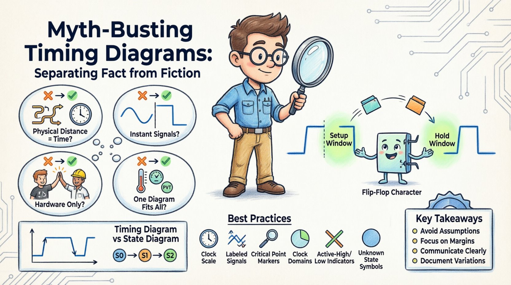
Myth 1: Timing Diagrams Show Exact Physical Distance 📏
The Fiction: Engineers often assume that the horizontal distance between two edges on a diagram directly correlates to physical trace length on a PCB.
The Fact: Timing diagrams represent logical or electrical time, not physical space. While trace length affects propagation delay, the diagram focuses on the result of that delay, not the geometry itself. A 1 nanosecond delay might represent a 15cm trace on a FR4 board or a 10cm trace on a copper trace with different dielectric constants. The diagram abstracts the physical medium to focus on the timing window.
- Physical length determines delay, but the diagram shows the delay value.
- Routing complexity is hidden; only the net result matters.
- Assuming a 1:1 scale between time and distance leads to layout errors.
Myth 2: Signal Transitions Are Instantaneous ⚡
The Fiction: In many diagrams, vertical lines indicate a signal changing state immediately.
The Fact: No physical signal changes state instantly. There is always a rise time and a fall time. When a diagram shows a vertical edge, it represents a transition that is fast relative to the clock period, but not zero. Ignoring transition times can lead to issues with signal integrity, such as ringing or crosstalk, which are not visible in idealized diagrams.
- Rise time is the duration to go from 10% to 90% of voltage.
- Diagrams often simplify this for readability, but simulation must account for it.
- High-speed designs require explicit modeling of transition slopes.
Myth 3: Timing Diagrams Are Only for Hardware Engineers 🛠️
The Fiction: Software developers and system architects often ignore timing diagrams, assuming they are irrelevant to code logic.
The Fact: Software must adhere to hardware timing constraints. Interrupts, DMA transfers, and memory-mapped I/O all depend on the timing established by the hardware. If a driver attempts to read data before the hardware asserts the “Ready” signal, a bus error occurs. Timing diagrams are essential for cross-disciplinary communication.
- Software interrupts must align with hardware clock cycles.
- Memory access windows are defined by timing specifications.
- Both hardware and software teams need a shared understanding of the timeline.
Myth 4: One Diagram Fits All Contexts 🌍
The Fiction: A single timing diagram can describe an entire system, regardless of operating conditions.
The Fact: Timing varies with temperature, voltage, and process variations (PVT). A diagram drawn for nominal conditions may fail at the extremes. Designers must account for worst-case scenarios. A diagram showing best-case behavior is often less useful than one highlighting the boundaries of operation.
- Worst-case delay determines the minimum clock period.
- Temperature affects resistance and capacitance.
- Process variation changes transistor switching speeds.
Deep Dive: Setup and Hold Times ⏱️
Understanding timing violations is critical. Two specific concepts dominate the analysis of data integrity: Setup Time and Hold Time. These are often the source of the most elusive bugs in digital systems.
Setup Time (Tsu)
Setup time is the minimum amount of time before a clock edge that data must be stable. If data changes too close to the clock edge, the receiving flip-flop may not capture the correct value.
- It ensures the data is settled before the capture window closes.
- Violations cause metastability or incorrect logic states.
- Path delay must be less than the clock period minus setup time.
Hold Time (Th)
Hold time is the minimum amount of time after a clock edge that data must remain stable. If data changes too soon after the clock edge, the flip-flop may lose the previously captured value.
- It ensures the data remains stable long enough to be latched.
- Violations are often harder to fix than setup violations.
- Path delay must be greater than the hold time requirement.
Timing Violation Scenarios
When analyzing a timing diagram, look for the following patterns:
- Setup Violation: The data signal is still changing when the clock edge arrives.
- Hold Violation: The data signal changes immediately after the clock edge.
- Glitch: A short pulse that falls within the setup/hold window but is not a valid transition.
Timing Diagram vs. State Diagram 🔄
Confusion often arises between timing diagrams and state diagrams. While both describe system behavior, they answer different questions. A state diagram shows what the system does (logic flow), while a timing diagram shows when it happens (temporal flow).
| Feature | Timing Diagram | State Diagram |
|---|---|---|
| Primary Focus | Time and Signal Levels | Logic and Control Flow |
| Axis Representation | Horizontal = Time | Horizontal = Logic States |
| Best For | Signal Integrity, Synchronization | Algorithm Design, FSM Logic |
| Complexity | High temporal detail | High logical branching |
| Signal Detail | Shows voltage levels (High/Low) | Shows abstract states (Idle/Run) |
Using the correct diagram for the task prevents miscommunication. A state machine can be designed without a timing diagram, but a high-speed bus interface cannot.
Best Practices for Creating Accurate Diagrams ✅
To ensure your documentation is effective, follow these guidelines. Precision in documentation reduces ambiguity in implementation.
- Define the Time Scale: Always specify the units (ns, µs, cycles). If using cycles, define the clock frequency.
- Label Every Signal: Do not use generic names like “Signal 1”. Use descriptive names like “CLK_IN” or “DATA_VALID”.
- Mark Critical Points: Highlight setup and hold windows explicitly with shading or annotations.
- Include Clock Domains: If multiple clocks exist, clearly distinguish them. Show the relationship between asynchronous clocks if applicable.
- Show Active High/Low: Clarify if an active state is High (1) or Low (0) to avoid polarity errors.
- Indicate Unknown States: Use X or Z to represent undefined or high-impedance states rather than leaving them blank.
Handling Asynchronous Signals 🔄
One of the most challenging aspects of timing diagrams is handling asynchronous signals. These are signals not synchronized to the main system clock. They introduce uncertainty that must be managed.
- Metastability: When an asynchronous signal arrives near a clock edge, the flip-flop may enter a metastable state. It will eventually resolve to 0 or 1, but the time taken is unpredictable.
- Synchronizers: Use chains of flip-flops to resolve metastability. Timing diagrams should show the metastable region resolving before the next clock edge.
- Handshaking: Protocols like I2C or SPI use asynchronous handshaking. The timing diagram must show the wait states where the master waits for the slave.
Real-World Application: Debugging a Race Condition 🐞
Imagine a scenario where a data bus is not being read correctly. The system hangs occasionally. A timing diagram analysis reveals the issue.
- Observation: The “Ready” signal is asserted slightly after the “Read” strobe.
- Diagram Check: The timing diagram shows the “Ready” edge falling within the setup window of the “Read” strobe.
- Conclusion: The data is being read before it is valid.
- Fix: Adjust the logic to delay the “Read” strobe or extend the “Ready” pulse.
This example highlights why visualizing the timeline is crucial. Without the diagram, the race condition remains hidden in the code logic.
Tools and Analysis Methods 🔍
While specific software names are not the focus, the methodologies for analysis remain constant. Modern engineering relies on simulation and waveform viewers to validate timing diagrams.
- Simulation: Run testbenches to generate waveforms that match the design intent.
- Static Timing Analysis (STA): Calculate delays without simulation to check for violations across all paths.
- Hardware Debugging: Use oscilloscopes to capture real-world waveforms and compare them against the theoretical diagram.
- Version Control: Keep timing diagrams in version control. Changes in hardware often require updates to the timing specifications.
The Impact of Jitter and Skew 📉
Timing diagrams are often drawn with perfect, straight lines. Reality is messier. Jitter and skew are noise sources that affect timing accuracy.
- Jitter: Variations in the timing of a signal’s edges. Clock jitter causes the sampling window to move.
- S skew: The difference in arrival time of the same clock signal at different points in the circuit.
- Impact: Both reduce the timing margin. A timing diagram should ideally show the margin, not just the ideal edge.
Summary of Key Takeaways 📝
Timing diagrams are more than just drawings; they are specifications of behavior. By understanding the myths and facts surrounding them, engineers can design more robust systems.
- Avoid Assumptions: Do not assume instant transitions or perfect synchronization.
- Focus on Margins: Setup and hold times are the safety buffers that prevent failure.
- Communicate Clearly: Use diagrams to bridge the gap between hardware and software teams.
- Document Variations: Acknowledge that timing changes with environment and process.
When you look at a timing diagram, see the time. See the constraints. See the reliability. This perspective transforms a static image into a powerful tool for engineering excellence.