


Timing diagrams are the backbone of digital system design. They provide a visual language that engineers use to describe how signals change over time. Whether you are designing a microcontroller interface or debugging a communication protocol, understanding these diagrams is essential. This guide walks you through the process of creating and interpreting them without unnecessary complexity.
Getting started might feel daunting, but with the right framework, you can draw effective diagrams quickly. We will cover the core components, the logic behind signal transitions, and the critical parameters that define system reliability. Let’s dive into the mechanics of signal timing.
Understanding the Core Purpose 🧠
A timing diagram is a graphical representation of the sequence of events in a system. It maps the state of signals against a common time axis. Unlike schematic diagrams that show physical connections, timing diagrams focus on temporal relationships. This distinction is crucial for debugging logic errors that do not appear in static circuit analysis.
When you draw these diagrams, you are documenting the behavior of data and control signals. The goal is to ensure that one signal is ready before another acts upon it. This synchronization prevents data corruption and ensures stable operation.
Visual Clarity: They make abstract time dependencies concrete.
Debugging Aid: They highlight race conditions and setup violations.
Documentation: They serve as a reference for hardware and software teams.
Verification: They help validate that logic matches specification.
Without a clear diagram, it is easy to miss subtle timing issues that only occur under specific conditions. By standardizing the way you draw, you reduce ambiguity for everyone involved in the project.
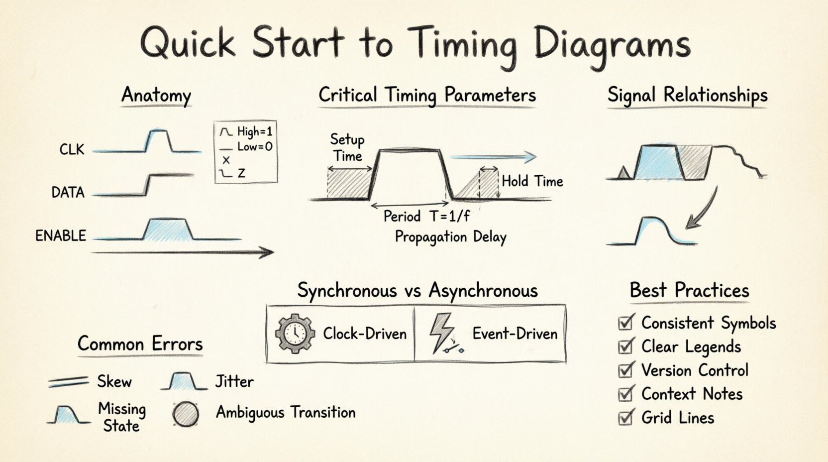
Anatomy of a Timing Diagram 📐
Every timing diagram shares a common structure. Mastering this structure allows you to read complex waveforms with ease. The layout is consistent across different engineering disciplines, from embedded systems to high-speed networking.
1. The Time Axis ⏰
The horizontal axis represents time. It flows from left to right. Time is not always linear in every context, but in most standard diagrams, equal distances represent equal time intervals. You do not need to label every millisecond, but marking key intervals helps scale the information.
Direction: Always left to right.
Scale: Can be linear or logarithmic depending on the signal frequency.
Markers: Use vertical lines to denote specific events like clock edges.
2. The Signal Lines 📊
Signals are represented by horizontal lines stacked vertically. Each line corresponds to a specific wire or net in the circuit. The name of the signal usually appears on the left or right side of the line.
Grouping: Related signals, such as address and data lines, are often grouped together.
Labeling: Always label signals clearly to avoid confusion between similar names.
Order: Place the most significant signal at the top or bottom, depending on convention.
3. Logic Levels 🔋
Signals toggle between defined states. In digital logic, these are typically High and Low, or 1 and 0. The vertical position of the line indicates the state.
State | Common Notation | Physical Meaning |
|---|---|---|
High | 1, H, VCC | Positive voltage rail |
Low | 0, L, GND | Ground or zero voltage |
Unknown | X | Indeterminate state |
High Impedance | Z | Disconnected or floating |
Understanding these levels is the first step in reading the diagram. Transitions between these levels are where the action happens.
Critical Timing Parameters ⚙️
Timing is not just about drawing lines; it is about defining constraints. Certain parameters dictate how fast a signal can change and when it must be stable. These constraints are vital for ensuring the system functions correctly.
1. Setup Time ⏳
Setup time is the minimum amount of time a data signal must be stable before a clock edge arrives. If the data changes too close to the clock edge, the system may capture the wrong value. This is a critical constraint in synchronous systems.
Definition: Time before the active clock edge.
Violation: Causes metastability or incorrect data capture.
Design Rule: Ensure data is stable well before the clock triggers.
2. Hold Time ⏳
Hold time is the minimum amount of time a data signal must remain stable after the clock edge. If the signal changes too soon after the trigger, the receiving element might not latch the value correctly.
Definition: Time after the active clock edge.
Violation: Similar to setup time, leads to data errors.
Design Rule: Ensure signal does not toggle immediately after the clock.
3. Propagation Delay ⏱️
Propagation delay is the time it takes for a signal to travel from the input of a component to its output. No electronic component is instantaneous. This delay accumulates across multiple stages and must be accounted for in high-speed designs.
Source: Internal gate delays and wire length.
Impact: Limits the maximum operating frequency.
Measurement: Measured from 50% point of input to 50% point of output.
4. Period and Frequency 🔁
For clock signals, the period is the time between two consecutive identical points on the waveform (e.g., rising edge to rising edge). Frequency is the reciprocal of the period.
Period: T = 1 / f
Duty Cycle: Percentage of time the signal is high within one period.
Stability: Clock jitter affects the precision of timing.
Reading and Analyzing Signal Relationships 🔄
Once you understand the components, the next step is analyzing how signals interact. This is where the diagram becomes a diagnostic tool. You look for dependencies and potential conflicts.
1. Edge Triggering 📉
Most digital circuits trigger on specific edges of the clock. Some trigger on the rising edge, while others use the falling edge. You must identify which edge is active for each component in your system.
Rising Edge: Transition from Low to High.
Falling Edge: Transition from High to Low.
Both Edges: Some systems sample data on both transitions.
When drawing, use small triangles or notches to indicate which edge is active. This prevents confusion during implementation.
2. Data Valid Windows 🕒
Data is only valid within a specific window. Before the setup time, and after the hold time, the data line must not change. Outside of this window, the data is considered valid. Marking this window on your diagram clarifies expectations.
Window: Defined by Setup + Hold + Propagation Delay.
Violation: If data changes outside this window, errors occur.
Visual Cue: Use shaded regions to highlight valid data periods.
3. Asynchronous Signals 📡
Not all signals follow the clock. Asynchronous signals like interrupts or resets operate independently. They require careful handling in timing diagrams to show their priority and latency.
Priority: Interrupts often take precedence over clock cycles.
Latency: Note the delay between assertion and response.
Stability: Ensure asynchronous signals are stable for setup/hold requirements.
Synchronous vs Asynchronous Systems 📡
The distinction between synchronous and asynchronous design impacts how you construct your diagrams. Each approach has specific rules and conventions.
Feature | Synchronous | Asynchronous |
|---|---|---|
Control | Driven by a clock | Driven by events |
Prediction | Easy to predict timing | Harder to predict timing |
Complexity | Standardized logic | Handshake protocols |
Power | Higher due to clock | Often lower |
In a synchronous diagram, you will see a dominant clock line that aligns all other signals. In an asynchronous diagram, you will see handshakes and wait states. Both require precise timing documentation.
Common Errors and How to Avoid Them ⚠️
Mistakes in timing diagrams can lead to costly hardware revisions. Being aware of common pitfalls helps you draw cleaner, more accurate representations.
1. Ignoring Skew 📏
Skew is the difference in arrival time of a signal at different points. If you assume all signals arrive simultaneously, you might miss timing violations. Always account for wire length and load differences.
Check: Compare arrival times at different receivers.
Fix: Add delay buffers or adjust trace lengths.
Visual: Show slight offsets in parallel lines if skew is significant.
2. Overlooking Jitter ⚡
Jitter is the variation in the timing of a signal. A clock might not be perfectly periodic. In high-speed designs, jitter can eat into your timing margins. Represent jitter as a shaded area around the clock edge.
Source: Power supply noise or external interference.
Impact: Reduces the effective setup and hold time.
Visual: Use fuzzy lines or bands to indicate uncertainty.
3. Ambiguous Transitions 🔄
A transition that looks like a straight line might actually be a slope. Real signals do not change instantly. Drawing perfect vertical lines implies infinite speed, which is physically impossible.
Best Practice: Draw transitions with a slight slope if precision is required.
Convention: Vertical lines are acceptable for logical representation.
Clarity: Ensure the intent is clear regardless of slope.
4. Missing State Transitions 🚦
Complex state machines often have intermediate states that are not obvious. If you only draw the start and end states, you lose critical information about the sequence.
Detail: Show all relevant state changes.
Labels: Annotate states with their names or values.
Logic: Ensure the diagram reflects the actual logic flow.
Best Practices for Documentation 📝
To ensure your diagrams are useful for years, follow a consistent style. This makes them easier to maintain and share with other engineers.
Consistent Symbols: Use the same arrowheads and line styles throughout.
Clear Legends: Define any custom symbols or abbreviations used.
Version Control: Label diagrams with version numbers and dates.
Context: Include a brief description of the system being diagrammed.
Grid Lines: Use a grid to help align signals and mark time intervals.
Consistency reduces the cognitive load on anyone reading your work. It also makes it easier to spot anomalies when you review the diagram later.
Troubleshooting with Timing Analysis 🛠️
When a system fails, timing diagrams are often the first place to look. They help isolate whether the issue is logical or temporal.
1. Identifying Race Conditions 🏁
A race condition occurs when the output depends on the order of events. If two signals arrive at a gate at the same time, the result might be unpredictable. Timing diagrams reveal these overlaps.
Look for: Signals crossing simultaneously.
Resolution: Add buffering or reorder logic.
Prevention: Design with margins to avoid simultaneous transitions.
2. Detecting Glitches ⚡
Glitches are short pulses that occur due to propagation delays. They might trigger a flip-flop unintentionally. On a diagram, they appear as narrow spikes between stable levels.
Visual: Narrow pulses that do not match the clock period.
Fix: Use filtering or latch the signal on the stable edge.
Analysis: Check if the pulse width exceeds the hold time.
3. Verifying Bus Protocols 📡
Buses like I2C or SPI have strict timing requirements. The start and stop conditions, clock stretching, and data shifts must align perfectly. Timing diagrams are the standard way to verify these protocols.
Start/Stop: Verify the correct transition on the data line relative to the clock.
Stretching: Ensure the slave can hold the clock low for the required duration.
Data: Confirm data is stable during the clock high phase.
Final Thoughts on Signal Integrity 🎯
Creating accurate timing diagrams is a skill that improves with practice. It requires a deep understanding of how electronics behave over time. By following the guidelines above, you can create diagrams that are both informative and reliable.
Remember that these diagrams are communication tools. They bridge the gap between theory and implementation. When you draw a timing diagram, you are telling a story about how the system behaves. Make that story clear, precise, and consistent.
Focus on the essential parameters: setup, hold, delay, and skew. Keep the layout clean and the labels unambiguous. With these habits, you will find that drawing timing diagrams becomes a natural part of your design process, allowing you to get drawing in minutes rather than hours.