


In the intricate world of embedded engineering, timing is everything. A microcontroller might function perfectly in simulation but fail catastrophically on hardware due to a few nanoseconds of delay. This is where the timing diagram becomes an indispensable tool. These visual representations map out the behavior of signals over time, providing a clear snapshot of how components interact within a digital system. Whether you are debugging a communication failure or designing a new peripheral interface, understanding how to read and create timing diagrams is fundamental.
This guide covers the essential mechanics of signal timing, from the basic definitions to complex protocol interactions. We will explore how to interpret waveforms, construct accurate diagrams from measurement data, and identify common pitfalls that lead to system instability. By mastering these visual tools, you gain the ability to predict system behavior and validate designs before they ever leave the bench.
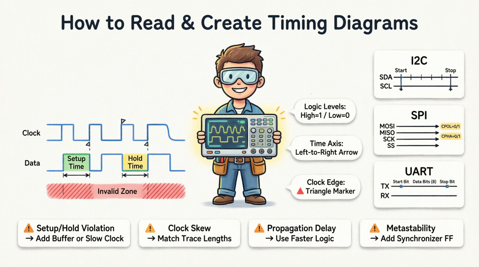
🔍 Understanding the Basics of Signal Timing
A timing diagram is not merely a drawing; it is a mathematical representation of logical states relative to a time axis. In embedded systems, we deal primarily with digital logic levels, which are binary: High (1) and Low (0). However, the transitions between these levels are where the complexity lies.
- Logic Levels: Most embedded systems operate on specific voltage thresholds. For example, a 3.3V system defines High as anything above 2.0V and Low as anything below 0.8V.
- Time Axis: Time flows from left to right. The horizontal spacing represents the duration of specific states or the delay between events.
- Signal Traces: Each horizontal line represents a specific wire or net. Multiple lines stacked vertically allow for the comparison of signal relationships.
When analyzing a system, you are looking for causality. Does the clock signal trigger the data change? Does the enable signal need to be active before the data is valid? Timing diagrams answer these questions visually.
🛠️ Key Components of a Timing Diagram
To interpret a diagram correctly, you must recognize the standard elements used to denote signal behavior. These components define the rules of engagement for the hardware.
| Component | Description | Visual Indicator |
|---|---|---|
| Signal Name | Identifies the specific wire or net | Text label on the left |
| Logic Level | High (1) or Low (0) state | Flat horizontal line at top or bottom |
| Transition Edge | Change from High to Low or vice versa | Vertical line connecting levels |
| Clock Edge | Trigger point for synchronous logic | Dashed line or triangle marker |
| Invalid Zone | Region where data cannot be read | Shaded or hatched area |
Understanding these components allows you to deconstruct complex interactions. For instance, a shaded area often indicates a setup or hold time requirement where the receiving device cannot reliably capture data.
👁️ How to Read a Timing Diagram Step-by-Step
Reading a timing diagram requires a systematic approach. You are essentially translating a visual pattern into a sequence of events. Follow this process to ensure accuracy.
1. Identify the Clock Source
Most embedded systems are synchronous, meaning a clock signal dictates the pace of operations. Locate the clock trace. It usually exhibits a regular, periodic square wave.
- Check the frequency. Is it 1 MHz or 100 MHz? This determines the speed of the entire system.
- Identify the edge type. Does the device trigger on the rising edge (Low to High) or the falling edge (High to Low)?
2. Map the Data Validity Windows
Data is only valid during specific windows relative to the clock. Look for the relationship between the clock edge and the data line.
- Setup Time: The data must be stable for a certain period before the clock edge.
- Hold Time: The data must remain stable for a certain period after the clock edge.
If the data changes during these windows, a timing violation occurs, leading to metastability or incorrect data capture.
3. Analyze Control Signals
Control signals like Chip Select (CS), Enable (EN), or Reset (RST) dictate when communication can occur.
- Is the Chip Select active low or active high?
- Does the Enable signal need to be asserted before the clock starts toggling?
- Are there any asynchronous events that override the clock logic?
4. Verify Handshaking Mechanisms
Many protocols use handshaking to manage flow control. Look for Acknowledge (ACK) or Ready (RDY) signals.
- Does the sender wait for a signal before transmitting the next byte?
- Are there timeout conditions represented in the diagram?
📐 How to Create Accurate Timing Diagrams
Creating a timing diagram is as critical as reading one. It serves as a specification for hardware engineers and a verification guide for software developers. You can generate these from requirements, measurement tools, or simulation data.
Step 1: Define the Protocol Requirements
Before drawing, gather the specifications. These usually come from the datasheet of the component you are interfacing with.
- Extract the minimum and maximum clock frequencies.
- Note the voltage levels for logic High and Low.
- Record the setup and hold time constraints.
Step 2: Capture Signal Data
Use hardware tools to capture real-world behavior. This ensures your diagram reflects reality rather than theoretical ideals.
- Oscilloscopes: Best for analog signal integrity and voltage levels.
- Logic Analyzers: Best for digital state transitions and multi-channel timing.
- Simulation Models: Good for verifying logic before hardware is available.
Step 3: Plot the Waveforms
Draw the signals chronologically. Ensure the time scale is consistent across all channels.
- Use straight lines for logic levels.
- Use diagonal lines for transitions to indicate rise and fall times.
- Label critical points such as the clock edge and data change.
Step 4: Annotate Critical Constraints
Annotations provide context that visuals alone cannot convey.
- Mark the setup and hold time windows explicitly.
- Indicate the duration of specific protocol states (e.g., Start Bit, Stop Bit).
- Highlight any known latency or delays in the signal path.
🌐 Timing Diagrams in Common Embedded Protocols
Different communication protocols have distinct timing characteristics. Understanding these nuances is vital for integration.
1. Inter-Integrated Circuit (I2C)
I2C is a two-wire synchronous serial bus. It uses SDA (Data) and SCL (Clock).
- Start Condition: SDA transitions from High to Low while SCL is High.
- Stop Condition: SDA transitions from Low to High while SCL is High.
- Data Transfer: Data is valid when SCL is High; changes occur when SCL is Low.
- ACK/NACK: The receiver pulls SDA Low during the ninth clock pulse to acknowledge receipt.
2. Serial Peripheral Interface (SPI)
SPI is a four-wire synchronous bus offering higher speeds than I2C.
- Lines: MOSI (Master Out), MISO (Master In), SCK (Clock), SS (Slave Select).
- CPOL: Clock Polarity determines the idle state (High or Low).
- CPHA: Clock Phase determines when data is sampled (first or second edge).
- Chip Select: Must be asserted (active) before the clock begins toggling.
3. Universal Asynchronous Receiver-Transmitter (UART)
UART is asynchronous, meaning there is no shared clock signal. Timing relies on baud rates.
- Start Bit: Pulls the line Low to signal the beginning of a frame.
- Data Bits: Transmitted LSB first, usually 8 bits.
- Stop Bit: Pulls the line High to signal the end of a frame.
- Parity: Optional bit for error checking.
| Feature | I2C | SPI | UART |
|---|---|---|---|
| Clock | Synchronous (Shared) | Synchronous (Shared) | Asynchronous (No Clock) |
| Wires | 2 (SDA, SCL) | 4+ (MOSI, MISO, SCK, SS) | 2 (TX, RX) |
| Addressing | Yes (Byte Address) | No (Wiring based) | No |
| Max Speed | ~400 kHz | ~50 MHz | ~3 Mbps |
⚠️ Common Timing Violations and Debugging
Even with careful design, timing violations can occur. These are often the root cause of intermittent bugs that are difficult to reproduce.
1. Setup and Hold Time Violations
These happen when data arrives too early or too late relative to the clock edge.
- Symptom: Data corruption or random errors in the logic analyzer capture.
- Fix: Slow down the clock speed or optimize the PCB trace lengths.
2. Clock Skew
Clock skew occurs when the clock signal arrives at different components at different times.
- Symptom: Race conditions where one flip-flop captures data before another is ready.
- Fix: Match trace lengths or use a dedicated clock distribution network.
3. Propagation Delay
Signals take time to travel through wires and gates. Long traces add significant delay.
- Symptom: Signal integrity issues or reflections on high-speed lines.
- Fix: Use termination resistors and keep traces as short as possible.
4. Metastability
When asynchronous signals cross clock domains, the receiving flip-flop may enter a metastable state.
- Symptom: System hangs or random resets.
- Fix: Use synchronizer chains (two or more flip-flops in series) to resolve the signal.
📝 Best Practices for Documentation
Creating timing diagrams for documentation ensures that future developers can understand the system without needing to reverse-engineer the hardware.
- Consistency: Use standard symbols and line styles across all diagrams in the project.
- Scale: Ensure the time axis is linear and clearly labeled with units (ns, µs, ms).
- Reference: Always link the diagram to the specific datasheet section or protocol standard.
- Clarity: Avoid clutter. If a signal is static, show it as a flat line rather than toggling noise.
- Versioning: Update diagrams whenever the hardware or firmware changes significantly.
🔗 Final Thoughts on Signal Integrity
Timing diagrams bridge the gap between abstract logic and physical reality. They allow engineers to visualize the invisible constraints of digital electronics. By learning to read them, you can troubleshoot complex hardware issues. By learning to create them, you can design robust systems that function reliably under all conditions.
The process involves patience and attention to detail. Every edge, every delay, and every voltage level matters. As embedded systems become faster and more complex, the reliance on precise timing diagrams will only increase. Treat them as critical specifications rather than optional documentation.
Start by analyzing the datasheets of the components you use. Look for the timing specifications. Then, try to draw the diagrams based on those numbers. Compare your drawings with actual measurements from your tools. This cycle of prediction and verification builds the intuition necessary for high-level embedded design.
Remember that a diagram is a tool for communication. It should convey the necessary information to another engineer with minimal ambiguity. Clear, accurate timing diagrams reduce development time and prevent costly hardware revisions. Invest the time to master this skill, and it will pay dividends throughout your engineering career.