


Digital systems rely on precise synchronization to function correctly. When signals arrive at the wrong moment, logic failures occur, leading to unpredictable behavior. Understanding how to analyze and correct these issues is essential for anyone studying digital logic, computer engineering, or electronics. This guide covers the core concepts and practical steps to identify and resolve timing problems encountered in sequential circuits and data transmission.
Understanding Clock Signals and Edges ⏱️
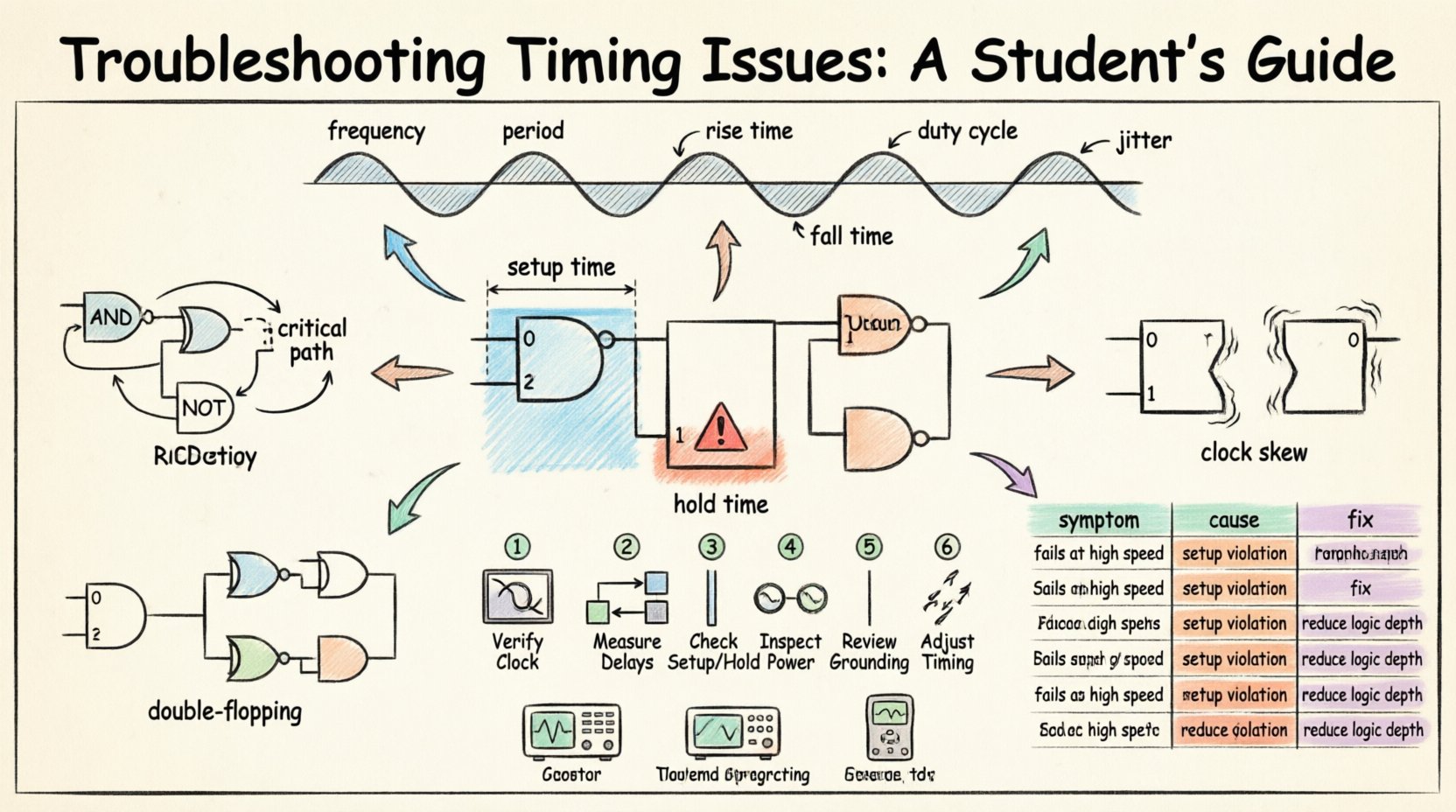
At the heart of most digital designs lies the clock signal. This periodic waveform dictates when data is sampled and when state changes occur. Troubleshooting often begins with verifying the integrity of this fundamental signal.
- Frequency and Period: The clock frequency determines the speed of operation. The period is the time duration of one full cycle. If the circuit requires a 100 MHz clock, the period is 10 nanoseconds. Any deviation here affects all downstream logic.
- Rise and Fall Times: A perfect square wave is theoretical. Real signals have finite rise and fall times. If the transition is too slow, the signal may spend too much time in the undefined voltage region, causing multiple toggles or logic errors.
- Duty Cycle: This is the ratio of time the signal is high versus the total period. A 50% duty cycle is standard, but some designs require asymmetric cycles. Deviations can skew timing margins for setup or hold requirements.
When inspecting a circuit, use an oscilloscope or logic analyzer to view the clock waveform. Look for noise spikes, ringing, or excessive jitter. Jitter refers to the deviation of the clock edge from its ideal position in time. High jitter reduces the effective timing margin available for data to settle.
Setup and Hold Time Violations ⚠️
These are the most common timing violations encountered in sequential logic design. Flip-flops and latches have specific requirements regarding when data must be stable relative to the clock edge.
Setup Time
Setup time is the minimum amount of time before the clock edge that data must be stable. If the data changes too close to the clock edge, the flip-flop may not capture the correct value.
- The Constraint: The propagation delay of the combinational logic feeding the flip-flop must be less than the clock period minus the setup time.
- The Symptom: The system might work at lower frequencies but fail as speed increases. Random bit errors often occur in the output.
- The Fix: Reduce the logic depth between registers, increase the clock period, or use faster components.
Hold Time
Hold time is the minimum amount of time after the clock edge that data must remain stable. If the data changes too soon after the clock edge, the flip-flop may lose the captured value.
- The Constraint: The propagation delay of the combinational logic must be greater than the hold time of the destination flip-flop.
- The Symptom: Hold violations often occur regardless of frequency. This is because the delay is absolute, not relative to the period.
- The Fix: Add delay buffers to the data path to slow the signal down, or redesign the logic to reduce delay.
It is crucial to distinguish between these two. Setup violations are frequency-dependent, while hold violations are path-dependent. A common mistake is trying to fix a hold violation by slowing the clock; this will not work and may make it worse.
Propagation Delays and Path Analysis 📉
Signals do not travel instantaneously. Every wire, gate, and component introduces a delay. Analyzing these delays is critical for ensuring data arrives on time.
- Combinational Logic Delay: This is the time taken for a signal to pass through gates like AND, OR, and NOT. Long chains of gates create significant latency.
- Interconnect Delay: On a physical board, wires have capacitance and resistance. Longer traces introduce more delay. This is often modeled as an RC network.
- Pin-to-Pin Delay: The time from a clock input to a data output in a component. This is usually specified in datasheets.
When troubleshooting, map out the critical path. This is the longest delay path between two sequential elements. If the critical path exceeds the clock period, the design will fail. To find it, calculate the sum of delays for all possible paths and identify the maximum.
Clock Skew and Jitter 📶
Even if the clock source is perfect, the signal might arrive at different components at different times. This phenomenon is known as skew.
- Clock Skew: This occurs when the clock signal travels different distances to reach different flip-flops. Positive skew delays the capture clock, relaxing setup time but tightening hold time. Negative skew tightens setup time but relaxes hold time.
- Clock Jitter: Short-term variations in the clock edge timing. Jitter reduces the timing budget available for data setup.
- Drift: Slow changes in clock frequency over time due to temperature or power supply fluctuations.
Skew is often managed by clock tree synthesis in complex designs. In student projects, it is usually minimized by routing clock traces evenly and keeping them short. If skew is suspected, measure the clock at multiple points in the circuit simultaneously.
Metastability and Asynchronous Inputs 🌀
When data changes at the same time as the clock edge, a flip-flop enters a metastable state. It does not settle to a 0 or 1 immediately but hovers in an intermediate voltage level.
- The Risk: Metastability can propagate through the system, causing logic errors that are difficult to reproduce.
- Asynchronous Signals: Inputs from external switches or communication ports often do not align with the internal clock. These must be synchronized.
- Double Flopping: A common technique to resolve metastability is passing the signal through two flip-flops in series. The first captures the metastable state, and the second resolves it during the next cycle.
Always treat asynchronous inputs as potential metastability sources. Do not connect them directly to logic that requires strict timing. Use synchronizer circuits to ensure safe data transfer between different clock domains.
A Step-by-Step Troubleshooting Workflow 🛠️
When a timing issue arises, follow a structured approach to isolate the cause. Random changes are unlikely to yield results.
- Verify the Clock: Check frequency, duty cycle, and amplitude. Ensure the signal is stable and clean.
- Measure Delays: Use a logic analyzer to capture input and output waveforms. Measure the actual propagation delay of the path.
- Check Setup and Hold: Calculate if the path satisfies the setup and hold constraints based on the measured delays.
- Inspect Power: Voltage drops can slow down gates. Ensure the power supply is stable and provides sufficient current.
- Review Grounding: Poor grounding can introduce noise that mimics timing errors. Check for ground loops and shared return paths.
- Adjust Timing: If the design is flexible, adjust the clock frequency or add buffers to balance the path.
Documentation is key during this process. Record the waveforms and measurements. This data helps in comparing expected behavior against actual performance.
Common Errors Reference Table 📊
Use this table as a quick reference for diagnosing specific symptoms.
| Observed Symptom | Probable Cause | Recommended Action |
|---|---|---|
| System fails at high speed | Setup Time Violation | Reduce logic depth or increase clock period |
| System fails at low speed | Hold Time Violation | Add delay buffers to data path |
| Random bit flips | Signal Noise or Jitter | Check shielding and power supply stability |
| Output hangs or resets | Metastability | Implement synchronizer chains |
| Inconsistent behavior | Clock Skew | Balance clock trace lengths |
| No output at all | Clock not enabled | Verify clock distribution and enable signals |
Tools and Instrumentation 📏
While simulation tools are useful, physical verification often requires specific hardware. Understanding how to use these instruments correctly is part of the troubleshooting skill set.
- Oscilloscope: Essential for viewing voltage levels and signal shape. Use high-impedance probes to avoid loading the circuit.
- Logic Analyzer: Better for digital signals. It captures the logic state (0 or 1) over time. It can trigger on specific patterns to isolate errors.
- Frequency Counter: Used to verify the exact frequency of the clock source if a scope is unavailable.
Ensure probes are compensated correctly. An uncompensated probe can distort the signal shape, leading to false conclusions about rise times and delays.
Final Considerations for Signal Integrity 🔒
Timing issues are often symptoms of broader signal integrity problems. As circuits become faster, the physical properties of the board matter more.
- Crosstalk: Signals on adjacent wires can interfere with each other. Keep high-speed lines separated from sensitive lines.
- Impedance Matching: If the trace impedance does not match the driver or receiver, reflections occur. These reflections can look like timing delays.
- Thermal Effects: As components heat up, their electrical characteristics change. This can alter propagation delays and lead to timing failures under load.
Designing for timing requires a holistic view. It is not just about logic gates; it is about the physical medium through which signals travel. By adhering to these principles, students can build robust systems that perform reliably under various conditions.
Regular practice with real hardware helps internalize these concepts. Theory provides the framework, but hands-on debugging builds the intuition needed to solve complex timing problems efficiently.