


In the intricate world of digital electronics and system design, communication between components relies heavily on precise temporal relationships. A timing diagram serves as the visual language that describes these relationships. It is a graphical representation that shows how signals change over time. Without this tool, debugging hardware interactions or verifying logic behavior would be nearly impossible. This guide explores the essential elements, parameters, and reading strategies required to interpret these diagrams effectively.
What Exactly Is a Timing Diagram? 📐
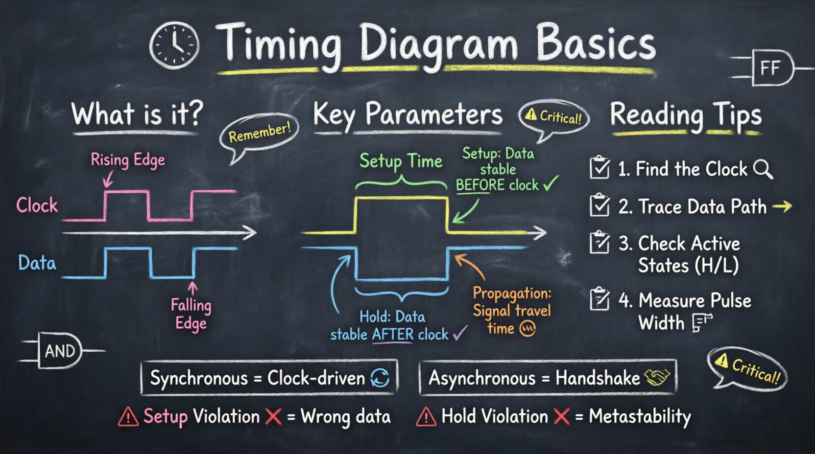
A timing diagram is a specific type of graph used to illustrate the relationship between two or more signals over a defined period. Unlike a logic state table, which lists states in a grid, a timing diagram maps these states onto a horizontal time axis. This visual approach allows engineers to see the sequence of events, the duration of pulses, and the synchronization between different parts of a circuit.
These diagrams are critical in several contexts:
- Hardware Design: To verify that data is stable before a clock edge arrives.
- Protocol Analysis: To understand communication standards like I²C, SPI, or UART.
- System Verification: To ensure state machines transition correctly without race conditions.
- Debugging: To identify setup or hold violations that cause system failures.
By visualizing the timing, designers can predict how a system behaves under load, ensuring reliability and performance.
Core Elements of a Timing Diagram 🎯
To read a timing diagram, one must first understand its fundamental building blocks. Every diagram consists of signals, time, and transitions. The arrangement of these elements tells a story about the electrical behavior of the system.
Signals and Lines
Each horizontal line represents a specific signal. This could be a clock signal, a data line, an address bus, or a control flag. Signals are typically labeled at the start of the line or in a legend. The vertical position of the line does not indicate voltage levels; rather, the vertical position relative to the baseline indicates logic states.
The Time Axis
The horizontal axis represents time. It flows from left to right. In many diagrams, time intervals are marked with vertical dashed lines. These markers often correspond to clock cycles. It is important to note that the time scale is not always linear. Sometimes, specific moments are zoomed in to show microsecond or nanosecond details, while other parts show macro-level behavior.
Logic Levels
Signals usually toggle between two states: High and Low. These correspond to binary 1 and 0. In some contexts, Low might represent an active state (Active Low), while High represents the active state (Active High). Understanding the active state is crucial for interpreting control signals like Reset or Chip Select.
Transitions and Edges
The vertical lines connecting the logic levels represent transitions. There are two primary types of edges:
- Rising Edge: A transition from Low to High.
- Falling Edge: A transition from High to Low.
These edges often trigger actions in digital circuits. For example, a register might update its data precisely when the clock signal rises.
Critical Timing Parameters ⚙️
Understanding the static lines is only half the battle. The dynamic parameters define the constraints within which the system must operate. Violating these parameters leads to data corruption or system crashes.
Setup Time
Setup time is the minimum amount of time before a clock edge that a data signal must be stable and valid. If the data changes too close to the clock edge, the receiving circuitry may not have enough time to register the value correctly. This parameter is strictly enforced in synchronous systems.
Hold Time
Hold time is the minimum amount of time after a clock edge that the data signal must remain stable. Even after the clock has triggered the capture, the data cannot change immediately. If it changes too quickly, the internal latch or flip-flop might enter an unstable state.
Propagation Delay
Propagation delay is the time it takes for a signal to travel from the input of a component to its output. This is inherent to the physical properties of the circuit. When multiple components are cascaded, these delays accumulate, affecting the maximum operating frequency of the system.
Clock Cycle and Frequency
The clock cycle is the duration of one complete period of the clock signal. Frequency is the inverse of this period, measured in Hertz (Hz). The timing budget of a system is often defined by the clock period. If the sum of all propagation delays exceeds the clock period, the system will fail to operate correctly.
| Parameter | Definition | Impact of Violation |
|---|---|---|
| Setup Time | Time data must be stable before clock edge | Missing data or incorrect capture |
| Hold Time | Time data must be stable after clock edge | Metastability or data corruption |
| Propagation Delay | Time for signal to travel through logic | Reduced max frequency or timing failure |
| Skew | Difference in arrival time of clock signal | Reduced timing margin |
| Jitter | Short-term variations in signal timing | Unstable operation at high speeds |
Reading and Analyzing Signals 📖
Interpreting a timing diagram requires a systematic approach. Rushing through the visual information can lead to misinterpretation of the system’s behavior. Follow these steps to analyze a diagram accurately.
- Identify the Clock: Locate the periodic signal that drives the system. This is usually the reference for all other actions.
- Trace the Data Path: Follow the signal lines from source to destination. Note where data is generated and where it is consumed.
- Check Active States: Determine if signals are active high or active low. A low signal might mean “Enable,” while a high signal might mean “Disable.”
- Measure Durations: Look at the width of pulses. Is the pulse wide enough to be detected? Is it too narrow to be a glitch?
- Verify Sequences: Ensure that control signals change in the correct order. For example, a Reset signal should be asserted before the system starts processing.
When analyzing complex diagrams, it helps to break the timeline into discrete cycles. Analyze one clock period at a time to understand the state transitions.
Synchronous vs. Asynchronous Systems 🔄
Timing diagrams differ significantly depending on whether the system is synchronous or asynchronous. Understanding this distinction is vital for correct interpretation.
Synchronous Systems
In a synchronous system, all operations are coordinated by a global clock. Every change in state occurs relative to a clock edge. This makes timing analysis more predictable. You can calculate the maximum speed of the system by summing the delays of the longest path between two registers. Timing diagrams here are highly regular, with events aligning vertically with clock edges.
Asynchronous Systems
Asynchronous systems do not rely on a global clock. Instead, they use handshaking protocols where signals change state based on the readiness of the previous stage. Timing diagrams for these systems appear less regular. Events are triggered by specific signal transitions rather than a periodic tick. Analyzing these requires careful attention to the dependency between signals.
Common Timing Issues and Violations ⚠️
Even with careful design, timing issues can arise. These problems often manifest as intermittent failures that are difficult to reproduce. Recognizing them in a timing diagram is a key skill for troubleshooting.
Setup Violations
A setup violation occurs when data arrives too late for the clock edge. Visually, this looks like the data transition happening after the clock edge has already passed. The result is often that the receiving component captures the wrong value or the previous value.
Hold Violations
A hold violation happens when data changes too soon after the clock edge. This means the new data overwrites the old data before the component has finished capturing it. This is particularly dangerous because it can lead to metastability, where the output voltage floats between high and low levels.
Skew and Jitter
Clock skew occurs when the clock signal arrives at different components at different times. If the skew is too large, the effective timing window for setup and hold is reduced. Jitter refers to the instability of the clock edge timing. High jitter makes it difficult to guarantee timing margins, requiring slower clock speeds.
Best Practices for Signal Integrity 🛡️
To ensure robust performance, engineers must adhere to best practices when designing and analyzing timing. These guidelines help minimize risks and improve system stability.
- Minimize Trace Lengths: Longer traces increase propagation delay and susceptibility to noise. Keep signal paths short where possible.
- Match Impedances: Ensure that the impedance of the transmission line matches the driver and receiver to prevent reflections.
- Use Ground Planes: A solid ground plane provides a low-impedance return path, reducing noise and crosstalk.
- Account for Temperature: Electronic components behave differently at various temperatures. Design margins should account for worst-case thermal conditions.
- Simulate Early: Use simulation tools to model timing behavior before physical prototypes are built. This catches violations early in the design cycle.
Application in Hardware Debugging 🔍
Timing diagrams are not just for design; they are essential tools for debugging. When a system fails, engineers use oscilloscopes or logic analyzers to capture the actual signal waveforms. These captured traces are then compared against the expected timing diagram.
If the actual waveform deviates from the diagram, the discrepancy points to the root cause. For instance, if a data line is noisy during the capture window, it indicates a power supply issue or electromagnetic interference. If the clock edge is sloped rather than sharp, it suggests a driver strength problem.
By correlating the visual data from the scope with the logical requirements of the timing diagram, engineers can pinpoint faults with precision. This process transforms abstract timing constraints into tangible physical evidence.
Summary of Key Concepts 💡
Mastering the basics of timing diagrams is fundamental to working with digital systems. It involves understanding the relationship between signals, time, and logic states. By paying close attention to parameters like setup time, hold time, and propagation delay, designers can create systems that operate reliably at high speeds.
The ability to read and interpret these diagrams allows for effective communication between hardware and software teams. It bridges the gap between theoretical logic and physical reality. Whether you are designing a simple control circuit or a complex microprocessor, timing analysis remains a cornerstone of engineering success.
Remember to always verify your active states, respect the clock boundaries, and account for physical limitations. With practice, interpreting these visual representations becomes second nature, enabling you to diagnose issues and optimize performance with confidence.