


Understanding the flow of signals over time is fundamental to digital electronics. For undergraduate engineers, mastering the interpretation of timing diagrams is not just an academic exercise; it is a critical skill for designing reliable systems. These visual representations map out the behavior of signals across a time axis, revealing relationships between clock cycles, data validity, and control signals. Without a firm grasp of these techniques, even simple circuits can fail under real-world conditions.
This guide covers the core principles required to read, create, and analyze timing diagrams effectively. We will explore the mechanics of synchronous and asynchronous design, the importance of setup and hold times, and how to avoid common pitfalls that lead to circuit failure. By the end of this article, you will have a solid foundation for tackling complex digital logic problems.
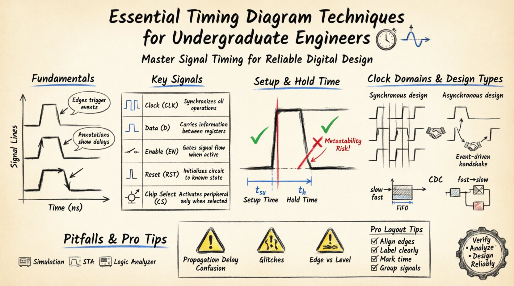
1. Fundamentals of Timing Diagrams 📐
A timing diagram is a graphical representation of signals over time. It allows engineers to visualize the state of various lines in a digital circuit. Unlike logic diagrams that show connectivity, timing diagrams show behavior. They are essential for debugging, verifying designs, and communicating signal interactions between hardware modules.
Key Components of a Timing Diagram
- Time Axis (X-Axis): Represents the progression of time. It is typically marked in nanoseconds (ns) or clock cycles.
- Signal Lines (Y-Axis): Horizontal lines representing individual wires or buses. Each line corresponds to a specific signal name.
- Logic Levels: Signals are generally binary, represented as High (1) or Low (0). Sometimes, ‘High-Z’ (High Impedance) states appear in bus designs.
- Edges: Vertical transitions indicate a change in state. Rising edges (Low to High) and falling edges (High to Low) are critical for triggering events.
- Annotations: Text labels often indicate delays, specific times, or conditions affecting the signal.
Why Timing Matters in Digital Logic
Digital systems rely on precise synchronization. If a signal arrives too early or too late relative to a clock edge, the system may misinterpret data. Timing diagrams make these constraints visible. They help answer questions like:
- Is the data stable before the clock edge?
- How long does a signal take to propagate through a gate?
- Do two clocks from different domains interfere with each other?
2. Key Signals and Components ⚡
Before analyzing complex waveforms, you must recognize the standard signals used in digital engineering. These signals dictate how data moves and when it is considered valid.
Common Signal Types
| Signal Name | Function | Typical Behavior |
|---|---|---|
| Clock (CLK) | Synchronization source | Pulsing regularly between 0 and 1 |
| Data (D) | Information carrier | Changes state based on input or logic |
| Enable (EN) | Activates a module | High to allow operation, Low to disable |
| Reset (RST) | Initializes state | Active Low or Active High pulse at start |
| Chip Select (CS) | Selects a device | Active Low to address specific component |
Understanding the active state of control signals is crucial. Some signals are active high, meaning they function when the voltage is high. Others are active low, indicated by a bar over the name (e.g., /RESET or RST_N), meaning they function when the voltage is low.
3. Setup and Hold Time Analysis 🕒
One of the most critical aspects of timing analysis involves setup and hold times. These parameters define the window in which data must be stable relative to a clock edge. Violating these constraints leads to data corruption or metastability.
Setup Time (tsu)
Setup time is the minimum duration that data must be stable before the active clock edge arrives. If the data changes too close to the clock edge, the flip-flop may not capture the correct value.
- Requirement: Data must be stable for tsu before the rising edge.
- Consequence of Violation: The register may capture incorrect data or enter an undefined state.
Hold Time (th)
Hold time is the minimum duration that data must remain stable after the active clock edge. The flip-flop needs a moment to latch the value before new data potentially arrives.
- Requirement: Data must remain stable for th after the rising edge.
- Consequence of Violation: Similar to setup violations, this causes data errors or metastability.
Visualizing Setup and Hold Times
When reading a timing diagram, look for the data signal relative to the clock edge. The data line should be flat and unchanging during the setup window (before) and the hold window (after). If the data line toggles within these windows, the design is likely flawed.
4. Clock Domain Crossing ⏱️
In complex systems, different parts of the circuit may operate at different clock speeds or frequencies. Moving data between these distinct clock domains is known as Clock Domain Crossing (CDC). This process introduces significant timing challenges.
Types of Clock Domains
- Same Frequency, Same Phase: Synchronous design. Simple timing analysis applies.
- Same Frequency, Different Phase: Requires phase alignment checks.
- Different Frequencies: Requires synchronization techniques like handshakes or FIFO buffers.
Handling CDC in Timing Diagrams
When analyzing diagrams with multiple clock domains, ensure you distinguish between the clock lines clearly. Data crossing from a slow domain to a fast domain can be risky if not managed. Conversely, fast to slow crossing can lead to data loss if the receiver samples too quickly.
- Handshake Protocols: Use valid/ready signals to confirm data transfer completion.
- FIFO Buffers: Decouple the production and consumption rates.
- Synchronizers: Use multi-stage flip-flops to reduce metastability risk.
5. Synchronous vs Asynchronous Design 🔄
Design architecture dictates how timing diagrams look. Understanding the difference helps in predicting signal behavior.
Synchronous Design
Most digital logic is synchronous. All state changes occur on the edge of a central clock signal.
- Predictability: Easier to analyze because timing is controlled.
- Timing Diagrams: Regular, grid-like patterns. Data changes align with clock edges.
- Limitations: Clock skew can become an issue in large designs.
Asynchronous Design
State changes occur based on the arrival of signals, not a global clock. This is common in handshake protocols and interrupt handling.
- Flexibility: Can be faster for specific tasks as it waits only for data.
- Timing Diagrams: Irregular. Signals depend on previous events, not fixed time slots.
- Risks: Prone to race conditions and hazards if not carefully designed.
6. Common Pitfalls and Errors ❌
Even experienced engineers make mistakes when interpreting or creating timing diagrams. Being aware of these common errors can save significant debugging time.
1. Ignoring Propagation Delay
Signals do not change instantaneously. Gates have a propagation delay. If you draw a diagram assuming immediate changes, your simulation will not match reality.
- Fix: Always include delay values between logic transitions in your diagrams.
2. Misinterpreting Active Low Signals
A signal labeled /CS is low when active. If you assume it is high, your logic will be inverted.
- Fix: Check the datasheet or schematic for active states. Look for bubbles on logic gates.
3. Overlooking Glitches
Glitches are short, unintended pulses. They can occur when signals travel through different paths with varying delays.
- Fix: Use hazard-free logic or add filtering stages in the design.
4. Confusing Edge vs Level
Some circuits trigger on the rising edge, others on the falling edge, and others on the level itself.
- Fix: Verify the trigger condition in the component specification.
7. Reading and Creating Professional Diagrams 📝
Clear communication is vital in engineering. A well-drawn timing diagram conveys complex information at a glance. Here are best practices for creating them.
Best Practices for Layout
- Align Edges: Ensure related signals change at consistent intervals.
- Label Clearly: Use signal names, not just generic lines.
- Mark Time: Indicate the duration of cycles or specific delays.
- Group Signals: Organize related signals (like data bus lines) together.
Step-by-Step Creation Process
- Identify Clocks: Draw the clock lines first. They are the backbone of the timing.
- Add Control Signals: Place enable, reset, and chip select lines.
- Plot Data: Add data lines based on the logic flow.
- Annotate: Add notes for setup/hold times or specific delays.
- Review: Check for violations and logical consistency.
8. Analyzing Real-World Scenarios 🔍
Let’s consider a scenario involving a memory read operation. This is a common task for engineers working with microcontrollers.
Memory Read Cycle
In a memory read, the processor sends an address, asserts a read command, and waits for data.
- Address Bus: Valid before the clock edge.
- Chip Select: Goes Low to activate the memory.
- Read Command: Goes Low to initiate the transfer.
- Data Bus: Remains in High-Z until the memory drives it.
- Timing: The data must be stable before the processor samples it.
Signal Integrity Considerations
As frequency increases, signal integrity becomes a major factor. Reflections, crosstalk, and noise can distort waveforms. Timing diagrams in high-speed designs must account for these physical layer issues.
- Slew Rate: How fast the signal transitions. Too fast causes noise; too slow causes timing errors.
- Voltage Levels: Ensure logic thresholds are met across temperature and voltage variations.
9. Advanced Timing Concepts 🧠
For those looking to deepen their expertise, several advanced concepts extend basic timing analysis.
Metastability
Metastability occurs when a flip-flop is unable to resolve to a stable 0 or 1 state within the required time. This usually happens when data changes too close to the clock edge.
- Probability: It is a probabilistic event, not deterministic.
- Mitigation: Use synchronizer chains (multiple flip-flops in series) to reduce the probability to near zero.
Clock Skew
Clock skew is the difference in arrival times of the clock signal at different parts of the circuit. Positive skew (arrives later) can help setup time but hurt hold time. Negative skew does the opposite.
- Design Impact: Skew must be accounted for in timing budgets.
- Measurement: Use oscilloscopes or simulation tools to measure skew.
Jitter
Jitter is the deviation of the clock edge from its ideal position. It reduces the effective setup and hold margins.
- Types: Period jitter, cycle-to-cycle jitter, and random jitter.
- Impact: High jitter limits the maximum operating frequency of a system.
10. Tools and Methodologies 🛠️
While manual analysis is educational, modern engineering relies on tools. However, understanding the underlying theory is what allows you to use these tools effectively.
Simulation Software
Hardware Description Languages (HDL) allow for simulation. These tools generate timing diagrams automatically from code. You must understand the output to verify the code’s correctness.
Static Timing Analysis (STA)
STA tools mathematically verify that all paths meet timing requirements without simulation. They check setup and hold violations across all corners (temperature, voltage).
Debugging with Logic Analyzers
Hardware debuggers capture real signals from a board. They display timing diagrams that match reality, helping to identify physical layer issues that simulation might miss.
Conclusion 🏁
Timing diagrams are the language of digital signal behavior. They bridge the gap between abstract logic and physical reality. For undergraduate engineers, investing time in mastering these techniques pays dividends throughout your career. Whether you are designing a simple counter or a complex processor, the ability to read and analyze timing constraints is non-negotiable.
By focusing on setup and hold times, understanding clock domains, and avoiding common pitfalls, you build a robust foundation. Remember to always verify active states and account for propagation delays. As you progress, you will encounter more complex scenarios, but the core principles remain the same. Keep practicing diagram analysis, and your designs will become more reliable and efficient.
Continue to refine your skills by studying datasheets and examining real-world circuit waveforms. The field of digital engineering evolves rapidly, but the fundamentals of timing analysis remain constant.