


In the intricate landscape of digital hardware design, clarity is paramount. Engineers and designers rely on visual representations to communicate how signals behave over time. The timing diagram stands as one of the most critical tools for this purpose. It transforms abstract logic into a visual timeline, revealing the dance of high and low states across various components. However, as systems grow in complexity, these diagrams can become overwhelming. This guide explores a modular strategy to dissect and analyze timing diagrams effectively, ensuring precision and reliability in hardware verification.
Understanding the flow of data and control signals is essential for preventing functional failures. Whether you are designing a microcontroller interface or a high-speed communication protocol, the ability to read and create these diagrams separates a robust design from a fragile one. By adopting a structured, modular perspective, teams can manage complexity and reduce the risk of timing violations.
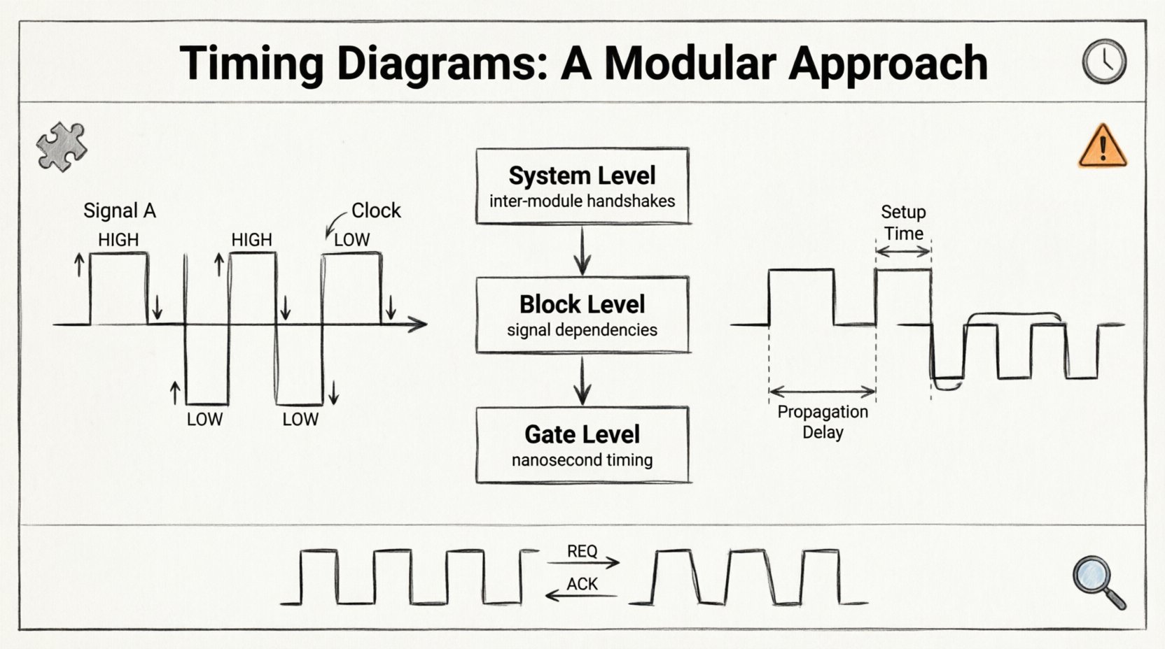
Understanding the Basics of Timing Diagrams ⏱️
A timing diagram is a graphical representation of how signals change state over time. It plots time on the horizontal axis and signal states on the vertical axis. This visual format allows engineers to verify the relationship between different signals within a digital circuit. The primary goal is to ensure that data is stable and valid when it is sampled by the receiving component.
Several key elements make up the foundation of any timing diagram:
- Signal Lines: Horizontal lines represent individual wires or buses carrying specific signals like clock, data, or control.
- Time Axis: The horizontal progression indicates the passage of time, often marked in nanoseconds or clock cycles.
- Logic Levels: Signals are typically binary, represented as High (1) or Low (0). Sometimes, undefined states or high-impedance states are also shown.
- Transitions: Vertical lines indicate the moment a signal switches from one state to another, such as rising or falling edges.
- Annotations: Text labels often define specific constraints, delays, or functional blocks within the diagram.
Without a clear understanding of these basics, interpreting complex interactions becomes difficult. A timing diagram is not merely a drawing; it is a contract between the transmitter and the receiver. It dictates the rules under which data must travel to be processed correctly.
The Modular Strategy for Complex Designs 🧩
Modern digital systems are rarely simple. They consist of multiple sub-systems, each with its own timing requirements. Attempting to draw the entire system in one diagram often leads to clutter and confusion. A modular approach breaks the design down into manageable chunks. This method enhances readability and simplifies the debugging process.
Why Modularity Matters
Breaking a system into modules allows designers to focus on specific interfaces without getting lost in the noise of the entire architecture. When a timing violation occurs, a modular diagram makes it easier to isolate the source of the problem. It reduces cognitive load and facilitates collaboration between different engineering teams working on separate blocks.
The benefits of this approach include:
- Isolation of Issues: Problems can be identified within a specific block rather than the whole system.
- Reusability: Standardized timing patterns for common modules can be reused across different projects.
- Scalability: New features can be added as new modules without redrawing the entire diagram.
- Team Efficiency: Different teams can work on their respective timing diagrams simultaneously.
Defining Module Boundaries
To implement this strategy effectively, clear boundaries must be established. Every module should have defined inputs and outputs. The timing diagram for a single module should focus on the signals crossing that boundary. Internal details can be abstracted away unless they directly impact the interface timing.
| Module Level | Focus Area | Detail Granularity |
|---|---|---|
| System Level | Inter-module communication | High-level handshakes |
| Block Level | Internal data paths | Specific signal dependencies |
| Gate Level | Propagation delays | Exact nanosecond timing |
By organizing diagrams according to these levels, engineers can maintain a clear hierarchy of information. This structure ensures that the right level of detail is available for the right stage of the design process.
Decoding Signal States and Transitions 📊
Once the modular structure is in place, the next step is analyzing the specific signals. Not all signals behave the same way. Some are continuous, while others are edge-triggered. Understanding the nature of each signal is vital for accurate diagram construction.
Common signal categories include:
- Clock Signals: The heartbeat of the system. These are periodic and drive state changes. They usually have strict frequency and duty cycle requirements.
- Data Signals: The actual information being transferred. These must be stable during specific windows relative to the clock.
- Control Signals: Signals that enable or disable functionality, such as Chip Select or Enable.
- Reset Signals: Initialization signals that force the system into a known state.
Transitions on these lines are critical. A rising edge often triggers an action, while a falling edge might complete it. In asynchronous systems, the relationship between these edges is less predictable, requiring more detailed analysis.
Visualizing Propagation Delay
No signal changes instantly. Physical limitations cause propagation delay. When a signal leaves a component, it takes time to travel through the wire and arrive at the next component. Timing diagrams must account for this latency. If a diagram shows a signal changing at time T, the receiving end might not see it until T + Δt.
Ignoring propagation delay can lead to significant errors in simulation and implementation. Engineers must model these delays to ensure that setup and hold times are met throughout the entire path.
Critical Timing Constraints Explained ⚠️
The most common source of failure in digital design is timing violation. These violations occur when signals do not meet the required stability windows. Two primary constraints govern this behavior: setup time and hold time.
Setup Time
Setup time is the minimum amount of time data must be stable before the active clock edge. If data arrives too late, the flip-flop may not capture the correct value. This constraint is critical for determining the maximum operating frequency of a system. If the clock period is shorter than the propagation delay plus the setup time, the system will fail.
Key considerations for setup time include:
- Longest path analysis is required to find the worst-case scenario.
- Process, voltage, and temperature variations affect delay.
- Clock jitter can eat into the available setup window.
Hold Time
Hold time is the minimum amount of time data must remain stable after the active clock edge. If the data changes too soon, the flip-flop might capture the wrong value or enter a metastable state. Unlike setup time, hold time is independent of the clock frequency. It depends on the internal delay of the component and the external path.
Hold time violations are often harder to fix because they cannot be resolved by slowing down the clock. Instead, they require adding delay to the data path or redesigning the logic.
Timing Constraint Summary
| Constraint | Definition | Impact on Frequency | Resolution Method |
|---|---|---|---|
| Setup Time | Stable before clock edge | Limits max frequency | Optimize logic path |
| Hold Time | Stable after clock edge | Independent of frequency | Add buffer delay |
| Propagation Delay | Time to travel through logic | Affects both | Circuit optimization |
Common Pitfalls and Violations 🚫
Even with a modular approach, errors can creep in. Recognizing common pitfalls helps prevent them during the design phase. Several types of violations are frequently encountered in hardware verification.
- Metastability: Occurs when a signal changes exactly at the clock edge. The flip-flop output becomes unpredictable. This is common when crossing clock domains.
- Glitches: Short, unintended pulses caused by logic path differences. These can trigger false state changes.
- Clock Skew: When the clock signal arrives at different components at different times. This reduces the effective timing window.
- Race Conditions: When the outcome depends on the sequence of events, which is unpredictable in asynchronous designs.
Addressing these issues requires careful analysis of the timing diagram. Look for overlapping windows where stability is not guaranteed. Ensure that reset sequences are followed correctly to avoid undefined states.
Implementing the Modular Workflow 🛠️
To effectively apply this methodology, follow a structured workflow. This ensures that every aspect of the timing is covered without redundancy.
- Define Interfaces: Clearly list all inputs and outputs for each module.
- Identify Clock Domains: Determine which signals belong to which clock domain.
- Map Data Paths: Trace the path from source to destination.
- Apply Constraints: Set setup and hold requirements for every flip-flop.
- Validate Transitions: Check edge alignments and pulse widths.
- Review Integration: Ensure module diagrams align when combined.
Each step builds upon the previous one. Skipping a step can lead to gaps in coverage. For instance, ignoring clock domains can result in synchronization failures that are difficult to debug later.
Handling Multi-Clock Domains 🌐
As designs grow, multiple clock frequencies become necessary. Some parts of the system run fast, while others run slow. Synchronizing these domains is one of the most challenging aspects of timing analysis.
When signals cross from one clock domain to another, the timing diagram must reflect the relationship between the two clocks. If the clocks are asynchronous, special care is needed to prevent metastability. Techniques such as synchronizer chains or handshake protocols are used to manage this transfer safely.
Key strategies for multi-clock designs include:
- Gray Coding: Using Gray codes to transmit multi-bit counters safely across domains.
- FIFO Buffers: Using First-In-First-Out queues to decouple read and write clocks.
- Handshake Signals: Using Request/Acknowledge pairs to ensure data validity.
Timing diagrams for these scenarios must explicitly show the clock edges of both domains. This allows engineers to see if the data remains stable long enough for the receiving clock to capture it.
Debugging with Visual Data 🔍
When a design fails, timing diagrams are the first place to look. Debugging requires patience and a systematic approach. Start by isolating the failing module. Compare the expected diagram against the actual waveform.
Look for discrepancies in:
- Signal timing relative to the clock.
- Pulse width of control signals.
- State transitions during reset.
- Glitches on data lines.
Tools often provide zooming capabilities to inspect nanosecond-level details. Use these features to verify the exact moment a violation occurs. Correlate the visual data with the logic to understand the root cause.
Final Thoughts on Design Integrity 💡
Timing diagrams are more than just technical drawings; they are the blueprint for reliable digital systems. By adopting a modular approach, engineers can manage complexity and maintain clarity. This method supports scalability and reduces the likelihood of costly errors.
Success in hardware design relies on attention to detail. Every nanosecond counts. Every transition matters. By rigorously applying these principles, teams can build systems that perform predictably under real-world conditions. The modular breakdown of timing analysis ensures that no detail is overlooked, leading to robust and efficient hardware solutions.
Continual refinement of these skills is necessary as technology advances. New standards and faster speeds require updated analysis techniques. Stay informed about emerging best practices to maintain a competitive edge in the field of digital engineering.