


When software engineers write code, they think in instructions, variables, and logic flows. When hardware engineers design circuits, they think in voltage levels, propagation delays, and clock cycles. These two worlds often exist in a state of friction. The code expects a signal to arrive at a specific logical moment, but the hardware operates on physical time, which is subject to noise, temperature, and electrical resistance. The bridge between these two domains is the timing diagram.
A timing diagram is not merely a picture; it is a contract. It defines the precise relationship between events in time. It tells the firmware when it is safe to read a pin and tells the silicon when it is safe to drive a line. Without a clear understanding of these diagrams, embedded systems fail unpredictably. Data corruption, race conditions, and system hangs become common issues. This guide explores the mechanics of timing diagrams, the physics behind them, and how to read and create them effectively.
📊 The Anatomy of a Signal
At its core, digital logic relies on binary states. In the physical world, however, these states are represented by voltage levels. A “High” might be 3.3 volts, and a “Low” might be 0 volts. But signals do not switch instantly. They rise and fall over a finite period. A timing diagram visualizes this transition.
Understanding the visual language of these diagrams is the first step toward mastery. Key elements include:
- Time Axis: Usually horizontal, moving from left to right. It can be linear or logarithmic, though linear is standard for most logic analysis.
- Signal Lines: Vertical lines representing specific wires, pins, or internal nodes.
- Transitions: The movement from Low to High (rising edge) or High to Low (falling edge). These edges often trigger state changes in sequential logic.
- Levels: The steady state of a signal before or after a transition.
- Labels: Text annotations that clarify the meaning of a specific pulse or interval.
Consider a simple clock signal. It oscillates between High and Low. The time it takes to complete one full cycle is the period. The inverse of the period is the frequency. In a timing diagram, the clock acts as the heartbeat of the system. Every other signal is often synchronized to these edges.
🕰️ The Clock Domain
Most digital systems operate within a clock domain. This is a group of circuits that share the same timing reference. However, signals often cross between different domains. This introduces complexity. A signal generated in a fast domain might arrive too late for a slow domain, or too early, causing a hold violation.
When analyzing timing, you must consider:
- Clock Skew: The difference in arrival time of the clock signal at different components. If the clock arrives at the sender before the receiver, timing margins shrink.
- Phase Shift: In some systems, signals are not aligned with the clock edge but occur in the middle of the cycle.
- Jitter: Variations in the timing of a signal. Jitter can be random or deterministic. It reduces the noise margin and makes the diagram less predictable.
Code written to interface with hardware assumes a stable clock. If the physical clock drifts due to temperature or voltage fluctuations, the timing diagram no longer matches the reality. This is why timing diagrams must include tolerance bands or worst-case scenarios.
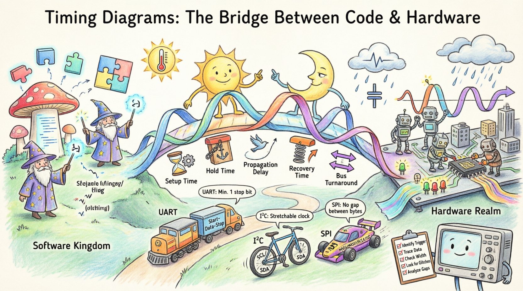
⚙️ Critical Timing Parameters
Specific parameters define the limits of signal integrity. These values are often found in datasheets but are best understood through the context of a timing diagram. The following table outlines the most critical parameters engineers must evaluate.
| Parameter | Definition | Impact on System |
|---|---|---|
| Setup Time | The minimum time data must be stable before the clock edge. | If violated, the receiving flip-flop cannot capture the correct value. |
| Hold Time | The minimum time data must remain stable after the clock edge. | If violated, the flip-flop may enter a metastable state. |
| Propagation Delay | Time taken for a signal to travel from input to output. | Delays accumulate across logic gates, potentially missing clock cycles. |
| Recovery Time | Time required for a control signal to return to normal after an asynchronous event. | Affects how quickly the system recovers from resets or interrupts. |
| Bus Turnaround Time | Time required to switch a bus from output mode to input mode. | Crucial for bidirectional buses like I2C or 1-Wire. |
Violating these parameters does not always cause an immediate crash. Sometimes the system works 99% of the time and fails only under specific conditions. This is why timing analysis is an iterative process. You must verify that the diagram holds true under worst-case voltage and temperature conditions.
👀 Reading the Waveform
Reading a timing diagram requires a systematic approach. When debugging a hardware issue, do not just look at the signal levels. Look at the relationships between signals.
Follow these steps to analyze a waveform:
- Identify the Trigger: Find the event that starts the sequence. This is usually a clock edge or an external interrupt.
- Trace the Data: Follow the data lines relative to the trigger. Does the data appear before or after the clock edge?
- Check the Width: Measure the duration of pulses. Is a “High” signal long enough to be recognized by the receiving logic?
- Look for Glitches: Spurious pulses that occur between stable states. These can be caused by crosstalk or logic hazards.
- Analyze the Gap: Look at the time between the end of one transaction and the start of the next. Is there enough time for the hardware to reset?
Often, the problem lies in the gap. If a microcontroller finishes writing data to a peripheral, it might need a specific delay before sending the next byte. If the diagram shows these bytes back-to-back without a gap, the code is likely too aggressive for the hardware.
🔌 Common Protocols and Timing
Different communication protocols impose different timing constraints. Understanding these constraints is essential for writing firmware that communicates reliably.
| Protocol | Key Timing Characteristic | Common Failure Mode |
|---|---|---|
| UART | Start bit followed by data bits and stop bit. Baud rate dependent. | Bit errors due to clock drift between sender and receiver. |
| I2C | SCL and SDA lines. Requires pull-up resistors. SDA must be stable during SCL High. | Bus hold-up or clock stretching issues causing timeouts. |
| SPI | Clock and Data lines are separate. Edge triggered (CPOL/CPHA settings). | Slaves responding too slowly for the master clock speed. |
| GPIO Interrupts | Edge sensitivity. Requires minimal processing time in ISR. | Missing interrupts due to long execution of previous service routines. |
For example, in SPI, the timing of the clock edge relative to the data line determines whether the data is latched on the rising or falling edge. If the firmware assumes one mode and the hardware is configured for the other, the data will be read incorrectly. A timing diagram clarifies this relationship visually, preventing configuration errors.
🔍 Debugging Issues with Timing
When a system behaves erratically, the first tool to reach for is not a debugger, but a timing diagram. Debugging with timing involves capturing the actual electrical behavior and comparing it to the expected design.
Common timing-related issues include:
- Metastability: When a signal arrives at a flip-flop too close to the clock edge, the output becomes unpredictable. It may settle to High, Low, or stay in an intermediate state for an indeterminate time.
- Race Conditions: When the outcome depends on the relative timing of events. If two signals change simultaneously, the order of processing matters.
- Signal Integrity: Reflections and ringing on long traces can cause false transitions. The diagram may show oscillations where a clean square wave should be.
- Setup/Hold Violations: The data changes too close to the clock edge. This is often caused by clock speed being too high for the logic path.
To resolve these, you may need to add delays in the code, change the clock frequency, or adjust the hardware layout. The timing diagram provides the evidence needed to make these changes confidently.
📝 Best Practices for Documentation
Creating timing diagrams for documentation is as important as reading them. Poorly documented timing leads to maintenance nightmares. Future engineers will struggle to understand why a specific delay was added to the code.
Follow these guidelines when creating your own diagrams:
- Use Standard Symbols: Avoid custom icons unless they are defined in a legend. Use standard rising/falling edge notation.
- Label Everything: Do not assume the reader knows what every line represents. Label pins, signals, and states clearly.
- Include Context: Show the state of control signals (like Chip Select or Enable) alongside data lines.
- Specify Units: Always indicate the time scale. Is it microseconds, nanoseconds, or clock cycles?
- Highlight Critical Paths: Use bold lines or different colors to emphasize the signals that determine system stability.
- Version Control: Update diagrams when the hardware or firmware changes. An outdated diagram is a liability.
Documentation should not just show the “happy path.” It should also show the error states. What does the diagram look like when a timeout occurs? What does it look like when a reset is triggered? These scenarios are often where the most bugs hide.
🌡️ Environmental Factors
A timing diagram is often generated under ideal laboratory conditions. Real-world environments are rarely ideal. Temperature, voltage, and electromagnetic interference all affect signal propagation.
Consider the following factors:
- Temperature: Silicon performance degrades at high temperatures. Propagation delay increases. A system that works at 25°C might fail at 85°C.
- Voltage: Lower supply voltage increases delay. Higher voltage might reduce delay but increases power consumption and heat.
- Load Capacitance: Long wires add capacitance. This slows down the rise and fall times of signals, effectively widening the pulse width but slowing the transition.
Robust design accounts for these variations. When creating a timing diagram for production, consider the “worst-case” corner. This means the diagram represents the slowest possible signal transitions and the fastest possible clock edges. If the system works under these conditions, it will work in most conditions.
🛠️ Creating and Validating Diagrams
While manual drawing is possible, modern engineering relies on automated tools to capture and validate timing. However, the principles remain the same regardless of the tool used. The goal is to visualize the flow of time.
When validating a diagram:
- Compare Against Datasheets: Ensure the timing values in your diagram match the manufacturer’s specifications for the chips used.
- Run Simulations: Use simulation environments to model the logic before building the physical circuit.
- Measure Real Hardware: Nothing replaces actual measurement. Capture waveforms from the physical board and overlay them on the design diagram.
- Check Margins: Is there enough slack time between signals? If the margin is zero, any variation will cause a failure.
Validation is an ongoing process. As firmware evolves, the timing requirements may change. A new interrupt handler might introduce a delay that pushes a signal past its deadline. Continuous verification ensures the bridge between code and hardware remains solid.
🔗 The Intersection of Logic and Physics
Ultimately, a timing diagram represents the intersection of logic and physics. Logic dictates what should happen; physics dictates what actually happens. The engineer’s job is to align these two realities.
By mastering the interpretation and creation of these diagrams, you gain the ability to diagnose complex failures that others might miss. You stop guessing why the system hangs and start seeing exactly where the timing constraint was violated. This level of insight transforms a developer into a designer.
Whether you are designing a simple sensor interface or a high-speed communication bus, the timing diagram is your primary reference. It ensures that the code you write executes in the time the hardware expects. It ensures that the signals you see on the screen match the voltages on the pins. It is the language of synchronization.
Invest time in understanding these diagrams. Treat them with the same seriousness as the code itself. In embedded systems, timing is not just a detail; it is the foundation of reliability. When the code and hardware speak the same language of time, the system performs with precision and stability.